
Technical Product Specification


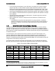

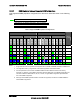
Table Of Contents
- 1. Introduction
- 2. Product Overview
- 3. Functional Architecture
- 3.1 Processor Support
- 3.1.1 Processor Population Rules
- 3.1.2 Multiple Processor Initialization
- 3.1.3 Enhanced Intel SpeedStep® Technology
- 3.1.4 Intel® Extended Memory 64 Technology (Intel® EM64T)
- 3.1.5 Execute Disable Bit Feature
- 3.1.6 Multi-Core Processor Support
- 3.1.7 Intel® Virtualization Technology
- 3.1.8 Platform Environmental Control Interface (PECI)
- 3.1.9 Common Enabling Kit (CEK) Design Support
- 3.2 Intel® 5400 Memory Controller Hub Chipset (Intel® 5400 MCH Chipset)
- 3.2.1 Processor Front-Side Buses
- 3.2.2 Snoop Filter
- 3.2.3 System Memory Controller and Memory Subsystem
- 3.2.3.1 Supported Memory
- 3.2.3.2 DIMM Population Rules and Supported DIMM Configurations
- 3.2.3.3 Minimum Memory Configuration
- 3.2.3.4 Memory upgrades
- 3.2.3.5 ECC Code Support
- 3.2.3.6 Memory Sparing
- 3.2.3.7 FBD Memory Thermal Management
- 3.2.3.8 BIOS Support of Memory Subsystem
- 3.2.3.9 Memory Error Handing
- 3.2.3.10 Memory Error Reporting
- 3.3 Intel® 6321ESB I/O Controller Hub
- 3.4 PCI Subsystem
- 3.4.1 Intel® 6321ESB I/O Controller Hub PCI32: 32-bit, 33-MHz PCI Bus Segment
- 3.4.2 Intel® 6321ESB I/O Controller Hub Port 1: x4 PCI Express* Bus Segment
- 3.4.3 Intel® 6321ESB I/O Controller Hub Port 2: x4 PCI Express* Bus Segment
- 3.4.4 MCH to Intel® 6321ESB I/O Controller Hub Chip-to-Chip Interface: Two x4 PCI Express* Bus Segments
- 3.4.5 MCH Ports 5-8: x16 Gen 2 PCI Express* Bus Segment
- 3.4.6 Scan Order
- 3.4.7 Resource Assignment
- 3.4.8 Automatic IRQ Assignment
- 3.4.9 Legacy Option ROM Support
- 3.4.10 EFI PCI APIs
- 3.4.11 Legacy PCI APIs
- 3.5 Video Support
- 3.6 Network Interface Controller (NIC)
- 3.7 Super I/O
- 3.1 Processor Support
- 4. Server Management
- 4.1 Intel® 6321ESB I/O Controller Hub Integrated Baseboard Management Controller (Integrated BMC) Feature Set
- 4.2 Advanced Configuration and Power Interface (ACPI)
- 4.3 System Initialization
- 4.4 Integrated Front Panel User Interface
- 4.5 Platform Control
- 4.6 Standard Fan Management
- 4.7 Private Management I2C Buses
- 4.8 Integrated BMC Messaging Interfaces
- 4.9 Event Filtering and Alerting
- 4.10 Watchdog Timer
- 4.11 System Event Log (SEL)
- 4.12 Sensor Data Record (SDR) Repository
- 4.13 Field Replaceable Unit (FRU) Inventory Device
- 4.14 Non-maskable Interrupt (NMI)
- 4.15 General Sensor Behavior
- 4.16 Processor Sensors
- 4.16.1 Processor Status Sensors
- 4.16.2 Processor VRD Over-temperature Sensor
- 4.16.3 ThermalTrip Monitoring
- 4.16.4 Internal Error (IERR) Monitoring
- 4.16.5 Dynamic Processor Voltage Monitoring
- 4.16.6 Processor Temperature Monitoring
- 4.16.7 Processor Thermal Control Monitoring (ProcHot)
- 4.16.8 CPU Population Error Sensor
- 4.17 Intel® Remote Management Module 2 (Intel RMM2) Support
- 5. System BIOS
- 5.1 BIOS Identification String
- 5.2 BIOS User Interface
- 5.2.1 Logo/Diagnostic Screen
- 5.2.2 BIOS Setup Utility
- 5.2.3 Server Platform Setup Utility Screens
- 5.2.3.1 Main Screen
- 5.2.3.2 Advanced Screen
- 5.2.3.3 Security Screen
- 5.2.3.4 Server Management Screen
- 5.2.3.5 Server Management System Information Screen
- 5.2.3.6 Boot Options Screen
- 5.2.3.7 Boot Manager Screen
- 5.2.3.8 Error Manager Screen
- 5.2.3.9 Exit Screen
- 5.3 Loading BIOS Defaults
- 5.4 Rolling BIOS
- 5.5 OEM Binary
- 6. Connector/Header Locations and Pin-outs
- 7. Jumper Block Settings
- 8. Intel® Light-Guided Diagnostics
- 9. Power and Environmental Specifications
- 9.1 Intel® Server Board S5400SF Design Specifications
- 9.2 Server Board Power Requirements
- 9.2.1 Processor Power Support
- 9.2.2 Power Supply DC Output Requirements
- 9.2.3 Power-on Loading
- 9.2.4 Grounding
- 9.2.5 Standby Outputs
- 9.2.6 Remote Sense
- 9.2.7 Voltage Regulation
- 9.2.8 Dynamic Loading
- 9.2.9 Capacitive Loading
- 9.2.10 Closed-Loop Stability
- 9.2.11 Common Mode Noise
- 9.2.12 Ripple/Noise
- 9.2.13 Soft Starting
- 9.2.14 Timing Requirements
- 9.2.15 Residual Voltage Immunity in Standby Mode
- 10. Regulatory and Certification Information
- Appendix A: Integration and Usage Tips
- Appendix B: POST Code Diagnostic LED Decoder
- Appendix C: POST Error Messages and Handling
- Appendix D: EFI Shell Commands
- Appendix E: Supported Intel® Server Chassis
- Appendix F: 1U PCI Express* Gen 2 Riser Card
- Glossary
- Reference Documents

Intel
®
Server Board S5400SF TPS Functional Architecture
Revision 2.02
Intel order number: D92944-007
19
3.2.1 Processor Front-Side Buses
The MCH supports two independent point-to-point processor front-side bus (FSB) interfaces.
Each front-side bus is 64 bits wide. Depending on the installed processor, the interfaces operate
using a 266 MHz,333 MHz, or 400 MHz clock, which is then quad pumped to support 1066 MT/s,
1333 MT/s, and 1600 MT/s transfer rates respectively. The following table provides the
theoretical bandwidth and transfer rates for each type of supported processor.
Table 5. Processor Front-Side Buses
FSB Clock (Quad pumped) FSB Transfer Rate FSB BW
266 MHz
(1066 MHz)
1066 MT/s 8 GB/s
333 MHz
(1333 MHz)
1333 MT/s 10.7 GB/s
400 MHz
(1600 MHz)
1600 MT/s 12.8 GB/s
The MCH supports 38-bit host addressing and decoding up to 128 GB of the processor’s
memory address space.
3.2.2 Snoop Filter
The MCH supports a 24 MB Snoop Filter (SF), which eliminates traffic on the snooped front-side
bus of the processor being snooped. By removing snoops from the snooped bus, the full
bandwidth is available for other transactions. Supporting concurrent snoops effectively reduces
performance degradation attributable to multiple snoop stalls.
The Snoop Filter has the following features:
Snoop Filter tracks total of 24 MB of processor L2 cache lines, this is equivalent to: (24 *
(2
20
) byte)/64 byte CL = 393,216 cache lines.
The SF is configured in 4 K sets organized as a 4 DID Affinity x 24 Way x 4 K Set -
Associativity array. This is equivalent to (2
12
Sets) x 24 Way x 4 DID = 393,216 tag
entries
4 x 24 Affinity Set - Associativity will allocate/evict entries within the 24-way
corresponding to the assigned affinity group if the SF look up is a miss. Each SF look up
will be based on 96-way (4x24 ways) look up.
The size of the snoop filter Tag RAM is: 4096 sets * 4 affinities * 24 ways *
33 bits/affinity/ set/way = 1,622,016 bytes
The size of the snoop filter Victim Ram is: 4096 sets * 4 affinities * 8 bits = 16,384 bytes
The size of the snoop filter Random ROM is: 1024 addresses * 16 bits = 2,048 bytes
The Snoop Filter is operated at 2x of the MCH core frequency, i.e., 533 MHz to provide
267 MLUU/s (where a Look-Up-Update operation is a read followed by a write operation
to the tag).
The maximum lookup and update bandwidth of the Snoop Filter is equal to the maximum
requested bandwidth from both FSBs. The lookup and update bandwidth from I/O
coherent transactions have to share the bandwidth with both FSBs per request
weighted-round-robin arbitration.