
Technical Product Specification

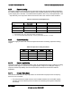
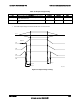
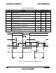

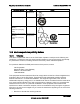
Table Of Contents
- 1. Introduction
- 2. Product Overview
- 3. Functional Architecture
- 3.1 Processor Support
- 3.1.1 Processor Population Rules
- 3.1.2 Multiple Processor Initialization
- 3.1.3 Enhanced Intel SpeedStep® Technology
- 3.1.4 Intel® Extended Memory 64 Technology (Intel® EM64T)
- 3.1.5 Execute Disable Bit Feature
- 3.1.6 Multi-Core Processor Support
- 3.1.7 Intel® Virtualization Technology
- 3.1.8 Platform Environmental Control Interface (PECI)
- 3.1.9 Common Enabling Kit (CEK) Design Support
- 3.2 Intel® 5400 Memory Controller Hub Chipset (Intel® 5400 MCH Chipset)
- 3.2.1 Processor Front-Side Buses
- 3.2.2 Snoop Filter
- 3.2.3 System Memory Controller and Memory Subsystem
- 3.2.3.1 Supported Memory
- 3.2.3.2 DIMM Population Rules and Supported DIMM Configurations
- 3.2.3.3 Minimum Memory Configuration
- 3.2.3.4 Memory upgrades
- 3.2.3.5 ECC Code Support
- 3.2.3.6 Memory Sparing
- 3.2.3.7 FBD Memory Thermal Management
- 3.2.3.8 BIOS Support of Memory Subsystem
- 3.2.3.9 Memory Error Handing
- 3.2.3.10 Memory Error Reporting
- 3.3 Intel® 6321ESB I/O Controller Hub
- 3.4 PCI Subsystem
- 3.4.1 Intel® 6321ESB I/O Controller Hub PCI32: 32-bit, 33-MHz PCI Bus Segment
- 3.4.2 Intel® 6321ESB I/O Controller Hub Port 1: x4 PCI Express* Bus Segment
- 3.4.3 Intel® 6321ESB I/O Controller Hub Port 2: x4 PCI Express* Bus Segment
- 3.4.4 MCH to Intel® 6321ESB I/O Controller Hub Chip-to-Chip Interface: Two x4 PCI Express* Bus Segments
- 3.4.5 MCH Ports 5-8: x16 Gen 2 PCI Express* Bus Segment
- 3.4.6 Scan Order
- 3.4.7 Resource Assignment
- 3.4.8 Automatic IRQ Assignment
- 3.4.9 Legacy Option ROM Support
- 3.4.10 EFI PCI APIs
- 3.4.11 Legacy PCI APIs
- 3.5 Video Support
- 3.6 Network Interface Controller (NIC)
- 3.7 Super I/O
- 3.1 Processor Support
- 4. Server Management
- 4.1 Intel® 6321ESB I/O Controller Hub Integrated Baseboard Management Controller (Integrated BMC) Feature Set
- 4.2 Advanced Configuration and Power Interface (ACPI)
- 4.3 System Initialization
- 4.4 Integrated Front Panel User Interface
- 4.5 Platform Control
- 4.6 Standard Fan Management
- 4.7 Private Management I2C Buses
- 4.8 Integrated BMC Messaging Interfaces
- 4.9 Event Filtering and Alerting
- 4.10 Watchdog Timer
- 4.11 System Event Log (SEL)
- 4.12 Sensor Data Record (SDR) Repository
- 4.13 Field Replaceable Unit (FRU) Inventory Device
- 4.14 Non-maskable Interrupt (NMI)
- 4.15 General Sensor Behavior
- 4.16 Processor Sensors
- 4.16.1 Processor Status Sensors
- 4.16.2 Processor VRD Over-temperature Sensor
- 4.16.3 ThermalTrip Monitoring
- 4.16.4 Internal Error (IERR) Monitoring
- 4.16.5 Dynamic Processor Voltage Monitoring
- 4.16.6 Processor Temperature Monitoring
- 4.16.7 Processor Thermal Control Monitoring (ProcHot)
- 4.16.8 CPU Population Error Sensor
- 4.17 Intel® Remote Management Module 2 (Intel RMM2) Support
- 5. System BIOS
- 5.1 BIOS Identification String
- 5.2 BIOS User Interface
- 5.2.1 Logo/Diagnostic Screen
- 5.2.2 BIOS Setup Utility
- 5.2.3 Server Platform Setup Utility Screens
- 5.2.3.1 Main Screen
- 5.2.3.2 Advanced Screen
- 5.2.3.3 Security Screen
- 5.2.3.4 Server Management Screen
- 5.2.3.5 Server Management System Information Screen
- 5.2.3.6 Boot Options Screen
- 5.2.3.7 Boot Manager Screen
- 5.2.3.8 Error Manager Screen
- 5.2.3.9 Exit Screen
- 5.3 Loading BIOS Defaults
- 5.4 Rolling BIOS
- 5.5 OEM Binary
- 6. Connector/Header Locations and Pin-outs
- 7. Jumper Block Settings
- 8. Intel® Light-Guided Diagnostics
- 9. Power and Environmental Specifications
- 9.1 Intel® Server Board S5400SF Design Specifications
- 9.2 Server Board Power Requirements
- 9.2.1 Processor Power Support
- 9.2.2 Power Supply DC Output Requirements
- 9.2.3 Power-on Loading
- 9.2.4 Grounding
- 9.2.5 Standby Outputs
- 9.2.6 Remote Sense
- 9.2.7 Voltage Regulation
- 9.2.8 Dynamic Loading
- 9.2.9 Capacitive Loading
- 9.2.10 Closed-Loop Stability
- 9.2.11 Common Mode Noise
- 9.2.12 Ripple/Noise
- 9.2.13 Soft Starting
- 9.2.14 Timing Requirements
- 9.2.15 Residual Voltage Immunity in Standby Mode
- 10. Regulatory and Certification Information
- Appendix A: Integration and Usage Tips
- Appendix B: POST Code Diagnostic LED Decoder
- Appendix C: POST Error Messages and Handling
- Appendix D: EFI Shell Commands
- Appendix E: Supported Intel® Server Chassis
- Appendix F: 1U PCI Express* Gen 2 Riser Card
- Glossary
- Reference Documents

Power and Environmental Specifications Intel
®
Server Board S5400SF TPS
Revision 2.02
Intel order number: D92944-007
148
2. The test setup uses an FET probe such as Tektronix* model P6046 or equivalent.
9.2.12 Ripple/Noise
The maximum allowed ripple/noise output of the power supply is defined in the following table.
This is measured over a bandwidth of 0 Hz to 20 MHz at the power supply output connectors. A
10 F tantalum capacitor in parallel with a 0.1 F ceramic capacitor are placed at the point of
measurement.
Table 89. Ripple and Noise
+3.3 V +5 V +12 V1/2/3/4 -12 V +5 VSB
50 mVp-p 50 mVp-p 120 mVp-p 120 mVp-p 50 mVp-p
9.2.13 Soft Starting
The power supply contains a control circuit that provides a monotonic soft start for its outputs
without overstress of the AC line or any power supply components at any specified AC line or
load conditions. The rise time of 5 VSB is from 1.0 ms to 25 ms and the turn on/off is monotonic.
9.2.14 Timing Requirements
The timing requirements for the power supply operation are as follows:
The output voltages must rise from 10% to within regulation limits (T
vout_rise
) within 5 to 70
ms, except for 5 VSB, in which case it is allowed to rise from 1.0 to 25 ms.
The +3.3 V, +5 V and +12 V output voltages should start to rise approximately at the
same time.
All outputs must rise monotonically.
The +5 V output needs to be greater than the +3.3 V output during any point of the
voltage rise.
The +5 V output must never be greater than the +3.3 V output by more than 2.25 V.
Each output voltage should reach regulation within 50 ms (T
vout_on
) of each other during
turn on of the power supply.
Each output voltage should fall out of regulation within 400 msec (T
vout_off
) of each other
during turn off.
Figure 52 and Figure 53 show the timing requirements for the power supply being turned on and
off via the AC input with PSON held low, and the PSON signal with the AC input applied.