
Technical Product Specification
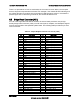
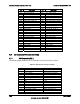


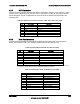

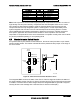
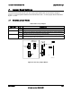
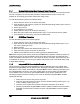
Table Of Contents
- 1. Introduction
- 2. Product Overview
- 3. Functional Architecture
- 3.1 Processor Support
- 3.1.1 Processor Population Rules
- 3.1.2 Multiple Processor Initialization
- 3.1.3 Enhanced Intel SpeedStep® Technology
- 3.1.4 Intel® Extended Memory 64 Technology (Intel® EM64T)
- 3.1.5 Execute Disable Bit Feature
- 3.1.6 Multi-Core Processor Support
- 3.1.7 Intel® Virtualization Technology
- 3.1.8 Platform Environmental Control Interface (PECI)
- 3.1.9 Common Enabling Kit (CEK) Design Support
- 3.2 Intel® 5400 Memory Controller Hub Chipset (Intel® 5400 MCH Chipset)
- 3.2.1 Processor Front-Side Buses
- 3.2.2 Snoop Filter
- 3.2.3 System Memory Controller and Memory Subsystem
- 3.2.3.1 Supported Memory
- 3.2.3.2 DIMM Population Rules and Supported DIMM Configurations
- 3.2.3.3 Minimum Memory Configuration
- 3.2.3.4 Memory upgrades
- 3.2.3.5 ECC Code Support
- 3.2.3.6 Memory Sparing
- 3.2.3.7 FBD Memory Thermal Management
- 3.2.3.8 BIOS Support of Memory Subsystem
- 3.2.3.9 Memory Error Handing
- 3.2.3.10 Memory Error Reporting
- 3.3 Intel® 6321ESB I/O Controller Hub
- 3.4 PCI Subsystem
- 3.4.1 Intel® 6321ESB I/O Controller Hub PCI32: 32-bit, 33-MHz PCI Bus Segment
- 3.4.2 Intel® 6321ESB I/O Controller Hub Port 1: x4 PCI Express* Bus Segment
- 3.4.3 Intel® 6321ESB I/O Controller Hub Port 2: x4 PCI Express* Bus Segment
- 3.4.4 MCH to Intel® 6321ESB I/O Controller Hub Chip-to-Chip Interface: Two x4 PCI Express* Bus Segments
- 3.4.5 MCH Ports 5-8: x16 Gen 2 PCI Express* Bus Segment
- 3.4.6 Scan Order
- 3.4.7 Resource Assignment
- 3.4.8 Automatic IRQ Assignment
- 3.4.9 Legacy Option ROM Support
- 3.4.10 EFI PCI APIs
- 3.4.11 Legacy PCI APIs
- 3.5 Video Support
- 3.6 Network Interface Controller (NIC)
- 3.7 Super I/O
- 3.1 Processor Support
- 4. Server Management
- 4.1 Intel® 6321ESB I/O Controller Hub Integrated Baseboard Management Controller (Integrated BMC) Feature Set
- 4.2 Advanced Configuration and Power Interface (ACPI)
- 4.3 System Initialization
- 4.4 Integrated Front Panel User Interface
- 4.5 Platform Control
- 4.6 Standard Fan Management
- 4.7 Private Management I2C Buses
- 4.8 Integrated BMC Messaging Interfaces
- 4.9 Event Filtering and Alerting
- 4.10 Watchdog Timer
- 4.11 System Event Log (SEL)
- 4.12 Sensor Data Record (SDR) Repository
- 4.13 Field Replaceable Unit (FRU) Inventory Device
- 4.14 Non-maskable Interrupt (NMI)
- 4.15 General Sensor Behavior
- 4.16 Processor Sensors
- 4.16.1 Processor Status Sensors
- 4.16.2 Processor VRD Over-temperature Sensor
- 4.16.3 ThermalTrip Monitoring
- 4.16.4 Internal Error (IERR) Monitoring
- 4.16.5 Dynamic Processor Voltage Monitoring
- 4.16.6 Processor Temperature Monitoring
- 4.16.7 Processor Thermal Control Monitoring (ProcHot)
- 4.16.8 CPU Population Error Sensor
- 4.17 Intel® Remote Management Module 2 (Intel RMM2) Support
- 5. System BIOS
- 5.1 BIOS Identification String
- 5.2 BIOS User Interface
- 5.2.1 Logo/Diagnostic Screen
- 5.2.2 BIOS Setup Utility
- 5.2.3 Server Platform Setup Utility Screens
- 5.2.3.1 Main Screen
- 5.2.3.2 Advanced Screen
- 5.2.3.3 Security Screen
- 5.2.3.4 Server Management Screen
- 5.2.3.5 Server Management System Information Screen
- 5.2.3.6 Boot Options Screen
- 5.2.3.7 Boot Manager Screen
- 5.2.3.8 Error Manager Screen
- 5.2.3.9 Exit Screen
- 5.3 Loading BIOS Defaults
- 5.4 Rolling BIOS
- 5.5 OEM Binary
- 6. Connector/Header Locations and Pin-outs
- 7. Jumper Block Settings
- 8. Intel® Light-Guided Diagnostics
- 9. Power and Environmental Specifications
- 9.1 Intel® Server Board S5400SF Design Specifications
- 9.2 Server Board Power Requirements
- 9.2.1 Processor Power Support
- 9.2.2 Power Supply DC Output Requirements
- 9.2.3 Power-on Loading
- 9.2.4 Grounding
- 9.2.5 Standby Outputs
- 9.2.6 Remote Sense
- 9.2.7 Voltage Regulation
- 9.2.8 Dynamic Loading
- 9.2.9 Capacitive Loading
- 9.2.10 Closed-Loop Stability
- 9.2.11 Common Mode Noise
- 9.2.12 Ripple/Noise
- 9.2.13 Soft Starting
- 9.2.14 Timing Requirements
- 9.2.15 Residual Voltage Immunity in Standby Mode
- 10. Regulatory and Certification Information
- Appendix A: Integration and Usage Tips
- Appendix B: POST Code Diagnostic LED Decoder
- Appendix C: POST Error Messages and Handling
- Appendix D: EFI Shell Commands
- Appendix E: Supported Intel® Server Chassis
- Appendix F: 1U PCI Express* Gen 2 Riser Card
- Glossary
- Reference Documents

Intel
®
Server Board S5400SF TPS Connector/Header Locations and Pin-outs
Revision 2.02
Intel order number: D92944-007
129
6.7.5 SATA Connectors
The server board provides six Serial ATA (SATA) connectors: SATA-0 (J1H1), SATA-1 (J1G2),
SATA-2 (J1G1), SATA-3 (J1F2), SATA-4 (J1F1), and SATA-5 (J1E2), for use with an internal
SATA backplane. The pin configuration for each connector is identical and is defined in the
following table.
Table 72. SATA Connector Pin-out (J1H1, J1G2, J1G1, J1F2, J1F1, J1E2)
Pin Signal Name Description
1 GND Ground
2 SATA#_TX_P_C Positive side of transmit differential pair
3 SATA#_TX_N_C Negative side of transmit differential pair
4 GND Ground
5 SATA#_RX_N_C Negative side of Receive differential pair
6 SATA#_RX_P_C Positive side of Receive differential pair
7 GND Ground
6.7.6 Serial Port Connectors
The server board provides one external RJ-45 Serial ‘B’ port (J9A2) and one internal 9-pin
Serial ‘A’ port header (J1B1). The following tables define the pin-outs for each.
Table 73. External RJ-45 Serial ‘B’ Port Pin-out (J9A2)
Pin Signal Name Description
1 SPB_RTS RTS (request to send)
2 SPB_DTR DTR (Data terminal ready)
3 SPB_OUT_N TXD (Transmit data)
4 GND Ground
5 SPB_RI RI (Ring Indicate)
6 SPB_SIN_N RXD (receive data)
7 SPB_DSR _DCD Data Set Ready/Data Carrier Detect
1
8 SPB_CTS CTS (clear to send)
Note: A jumper block on the server board determines whether DSR or DCD is routed to pin 7. The
board has the jumper block configured with DSR enabled at production.
Table 74. Internal 9-pin Serial ‘A’ Header Pin-out (J1B1)
Pin Signal Name Description
1 SPA_DCD DCD (carrier detect)
2 SPA_DSR DSR (data set ready)
3 SPA_SIN_L RXD (receive data)
4 SPA_RTS RTS (request to send)
5 SPA_SOUT_N TXD (Transmit data)
6 SPA_CTS CTS (clear to send)
7 SPA_DTR DTR (Data terminal ready)
8 SPA_RI RI (Ring Indicate)
9 GND Ground