
Technical Product Specification
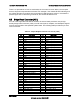
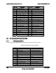


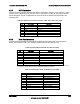

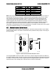
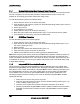
Table Of Contents
- 1. Introduction
- 2. Product Overview
- 3. Functional Architecture
- 3.1 Processor Support
- 3.1.1 Processor Population Rules
- 3.1.2 Multiple Processor Initialization
- 3.1.3 Enhanced Intel SpeedStep® Technology
- 3.1.4 Intel® Extended Memory 64 Technology (Intel® EM64T)
- 3.1.5 Execute Disable Bit Feature
- 3.1.6 Multi-Core Processor Support
- 3.1.7 Intel® Virtualization Technology
- 3.1.8 Platform Environmental Control Interface (PECI)
- 3.1.9 Common Enabling Kit (CEK) Design Support
- 3.2 Intel® 5400 Memory Controller Hub Chipset (Intel® 5400 MCH Chipset)
- 3.2.1 Processor Front-Side Buses
- 3.2.2 Snoop Filter
- 3.2.3 System Memory Controller and Memory Subsystem
- 3.2.3.1 Supported Memory
- 3.2.3.2 DIMM Population Rules and Supported DIMM Configurations
- 3.2.3.3 Minimum Memory Configuration
- 3.2.3.4 Memory upgrades
- 3.2.3.5 ECC Code Support
- 3.2.3.6 Memory Sparing
- 3.2.3.7 FBD Memory Thermal Management
- 3.2.3.8 BIOS Support of Memory Subsystem
- 3.2.3.9 Memory Error Handing
- 3.2.3.10 Memory Error Reporting
- 3.3 Intel® 6321ESB I/O Controller Hub
- 3.4 PCI Subsystem
- 3.4.1 Intel® 6321ESB I/O Controller Hub PCI32: 32-bit, 33-MHz PCI Bus Segment
- 3.4.2 Intel® 6321ESB I/O Controller Hub Port 1: x4 PCI Express* Bus Segment
- 3.4.3 Intel® 6321ESB I/O Controller Hub Port 2: x4 PCI Express* Bus Segment
- 3.4.4 MCH to Intel® 6321ESB I/O Controller Hub Chip-to-Chip Interface: Two x4 PCI Express* Bus Segments
- 3.4.5 MCH Ports 5-8: x16 Gen 2 PCI Express* Bus Segment
- 3.4.6 Scan Order
- 3.4.7 Resource Assignment
- 3.4.8 Automatic IRQ Assignment
- 3.4.9 Legacy Option ROM Support
- 3.4.10 EFI PCI APIs
- 3.4.11 Legacy PCI APIs
- 3.5 Video Support
- 3.6 Network Interface Controller (NIC)
- 3.7 Super I/O
- 3.1 Processor Support
- 4. Server Management
- 4.1 Intel® 6321ESB I/O Controller Hub Integrated Baseboard Management Controller (Integrated BMC) Feature Set
- 4.2 Advanced Configuration and Power Interface (ACPI)
- 4.3 System Initialization
- 4.4 Integrated Front Panel User Interface
- 4.5 Platform Control
- 4.6 Standard Fan Management
- 4.7 Private Management I2C Buses
- 4.8 Integrated BMC Messaging Interfaces
- 4.9 Event Filtering and Alerting
- 4.10 Watchdog Timer
- 4.11 System Event Log (SEL)
- 4.12 Sensor Data Record (SDR) Repository
- 4.13 Field Replaceable Unit (FRU) Inventory Device
- 4.14 Non-maskable Interrupt (NMI)
- 4.15 General Sensor Behavior
- 4.16 Processor Sensors
- 4.16.1 Processor Status Sensors
- 4.16.2 Processor VRD Over-temperature Sensor
- 4.16.3 ThermalTrip Monitoring
- 4.16.4 Internal Error (IERR) Monitoring
- 4.16.5 Dynamic Processor Voltage Monitoring
- 4.16.6 Processor Temperature Monitoring
- 4.16.7 Processor Thermal Control Monitoring (ProcHot)
- 4.16.8 CPU Population Error Sensor
- 4.17 Intel® Remote Management Module 2 (Intel RMM2) Support
- 5. System BIOS
- 5.1 BIOS Identification String
- 5.2 BIOS User Interface
- 5.2.1 Logo/Diagnostic Screen
- 5.2.2 BIOS Setup Utility
- 5.2.3 Server Platform Setup Utility Screens
- 5.2.3.1 Main Screen
- 5.2.3.2 Advanced Screen
- 5.2.3.3 Security Screen
- 5.2.3.4 Server Management Screen
- 5.2.3.5 Server Management System Information Screen
- 5.2.3.6 Boot Options Screen
- 5.2.3.7 Boot Manager Screen
- 5.2.3.8 Error Manager Screen
- 5.2.3.9 Exit Screen
- 5.3 Loading BIOS Defaults
- 5.4 Rolling BIOS
- 5.5 OEM Binary
- 6. Connector/Header Locations and Pin-outs
- 7. Jumper Block Settings
- 8. Intel® Light-Guided Diagnostics
- 9. Power and Environmental Specifications
- 9.1 Intel® Server Board S5400SF Design Specifications
- 9.2 Server Board Power Requirements
- 9.2.1 Processor Power Support
- 9.2.2 Power Supply DC Output Requirements
- 9.2.3 Power-on Loading
- 9.2.4 Grounding
- 9.2.5 Standby Outputs
- 9.2.6 Remote Sense
- 9.2.7 Voltage Regulation
- 9.2.8 Dynamic Loading
- 9.2.9 Capacitive Loading
- 9.2.10 Closed-Loop Stability
- 9.2.11 Common Mode Noise
- 9.2.12 Ripple/Noise
- 9.2.13 Soft Starting
- 9.2.14 Timing Requirements
- 9.2.15 Residual Voltage Immunity in Standby Mode
- 10. Regulatory and Certification Information
- Appendix A: Integration and Usage Tips
- Appendix B: POST Code Diagnostic LED Decoder
- Appendix C: POST Error Messages and Handling
- Appendix D: EFI Shell Commands
- Appendix E: Supported Intel® Server Chassis
- Appendix F: 1U PCI Express* Gen 2 Riser Card
- Glossary
- Reference Documents

Connector/Header Locations and Pin-outs Intel
®
Server Board S5400SF TPS
Revision 2.02
Intel order number: D92944-007
126
Pin Signal Name Pin Signal Name
KEY KEY
A37 BMC_RST_BTN_N B37 NIC2_LINK_LED_N
A38 FP_PWR_BTN_N B38 NIC2_ACT_LED_N
A39 FP_ID_BTN B39 LED_STATUS_AMBER_R1
A40 GND B40 GND
A41 SMB_IPMB_ 5VSB_SDA B41 SMB_SN_3V3SB_DAT_BUF
A42 SMB_IPMB_ 5VSB_CLK B42 SMB_SN_3V3SB_CLK_BUF
A43 GND B43 GND
A44 LED_ HDD_ACTIVITY_N B44 V_IO_HSYNC2_BUF_FP
A45 P3V3 B45 V_IO_VSYNC2_BUF_FP
A46 FP_PWR_LED_N_R B46 GND
A47 P3V3_STBY B47 V_IO_BLUE_CONN_FP
A48 FP_ID_LED_R1_N B48 V_IO_GREEN_CONN_FP
A49 FM_SIO_TEMP_SENSOR B49 V_IO_RED_CONN_FP
A50 LED_FAN3_FAULT B50 GND
A51 LED_FAN2_FAULT B51 LED_FAN10_FAULT
A52 LED_FAN1_FAULT B52 LED_FAN5_FAULT
A53 FAN_PWM_CPU1 B53 LED_FAN4_FAULT
A54 GND B54 FAN_IO_PWM
A55 FAN_PWM_CPU2 B55 GND
A56 PCI_FAN_TACH9 B56 PCI_FAN_TACH10
A57 FAN_TACH7 B57 FAN_TACH8
A58 FAN_TACH5 B58 FAN_TACH6
A59 FAN_TACH3_H7 B59 FAN_TACH4_H7
A60 FAN_TACH1_H7 B60 FAN_TACH2_H7
6.7 I/O Connector Pin-out Definition
6.7.1 VGA Connector (J6A1)
The following table details the pin-out definition of the VGA connector (J6A1).
Table 68. VGA Connector Pin-out (J6A1)
Pin Signal Name Description
1 V_IO_R_CONN Red (analog color signal R)
2 V_IO_G_CONN Green (analog color signal G)
3 V_IO_B_CONN Blue (analog color signal B)
4 TP_VID_CONN_B4 No connection
5 GND Ground
6 GND Ground
7 GND Ground
8 GND Ground
9 TP_VID_CONN_B9 No Connection
10 GND Ground
11 TP_VID_CONN_B11 No connection
12 V_IO_DDCDAT DDCDAT
13 V_IO_HSYNC_CONN HSYNC (horizontal sync)
14 V_IO_VSYNC_CONN VSYNC (vertical sync)
15 V_IO_DDCCLK DDCCLK