
Technical Product Specification


Server Board Power Distribution Intel® Server Board S1400FP TPS
Intel order number G64246-003 Revision 2.0
106
12.1.5
Dynamic Loading
The output voltages remain within limits specified for the step loading and capacitive loading
specified in the table below.
The load transient repetition rate is tested between 50Hz and 5kHz
at duty cycles ranging from 10%-90%.
The load transient repetition rate is only a test
specification.
The ∆ step load may occur anywhere within the MIN load to the MAX load
conditions.
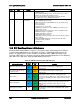
Table 56. Transient Load Requirements
Output
∆ Step Load Size
(See note 2)
Load Slew Rate
Test capacitive Load
+3.3V
6.0A
0.5 A/µsec
970 µF
+5V
4.0A
0.5 A/µsec
400 µF
12V1+12V2
18.0A
0.5 A/µsec
2200 µF
1,2
+5VSB
0.5A
0.5 A/µsec
20 µF
Notes:
1. Step loads on each 12V output may happen simultaneously.
2. The +12V should be tested with 2200µF evenly split between the four +12V rails.
3. This will be tested over the range of load conditions in section 12.1.2.
12.1.6
Capacitive Loading
The power supply is stable and meets all requirements with the following capacitive loading
ranges.
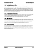
Table 57. Capacitive Loading Conditions
Output
MIN
MAX
Units
+3.3V
250
5000
µ
F
+5V
400
5000
µ
F
+12V
500
8000
µ
F
-12V
1
350
µ
F
+5VSB
20
350
µ
F
12.1.7
Grounding
The output ground of the pins of the power supply provides the output power return path.
The
output connector ground pins are connected to the safety ground (power supply enclosure).
This
grounding is well designed to ensure passing the max allowed Common Mode Noise levels.
The power supply is provided with a reliable protective earth ground. All secondary circuits are
connected to protective earth ground. Resistance of the ground returns to chassis does not
exceed 1.0 mΩ. This path may be used to carry DC current.
12.1.8
Residual Volatge Immunity in Standy mode
The power supply is immune to any residual voltage placed on its outputs (Typically a leakage
voltage through the system from standby output) up to 500mV. There is neither additional heat
generated, nor stressing of any internal components with this voltage applied to any individual
or all outputs simultaneously.
It also does not trip the protection circuits during turn on.
The residual voltage at the power supply outputs for no load condition does not exceed 100mV
when AC voltage is applied and the PSON# signal is de-asserted.