
Technical Product Specification


Power Subsystem Intel® Server System R2000IP Product Family TPS
30 Revision 1.1
regulation limits or when AC power has been removed for a time sufficiently long so that power
supply operation is no longer guaranteed, PWOK will be de-asserted to a LOW state. The start
of the PWOK delay time shall inhibited as long as any power supply output is in current limit.
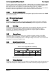
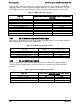
Table 26. PWOK Signal Characteristics
Signal Type
Open collector/drain output from power supply. Pull-up to +3.3V located in the
power supply.
PWOK = High
Power OK
PWOK = Low
Power Not OK
MIN
MAX
Logic level low voltage
0V
0.4V
Logic level high voltage
2.4 V
3.46 V
Sink current, PWOK = low
400uA
Source current, pull-up resistor
2mA
PWOK delay: T
pwok_on
100 ms
1000 ms
PWOK rise and fall time
100 s
Power down delay: T
pwok_off
1 ms
200ms
3.8.4 A0, A1 Address Assignment Output Signal
A0 and A1 are dedicated to assignment the address for power supplies. See the table below for
representation of the characteristics of A0 and A1.
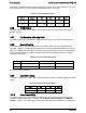
Table 27. A0 and A1 Signal Characteristics
Signal Type
Input, Pull-up to +3.3V located in power supply.
MIN
MAX
Logic level low voltage
0V
0.4V
Logic level high voltage
2.4 V
3.46 V
Source current, pull-up resistor
2mA
3.8.5 SCL and SDA Output Signals
SCL and SDA signals are tied to pull-up to +3.3V internal to the power supply with 49.9k
resistors to prevent floating signals. Pull-up resistors are required on the system for proper
operation.
Table 28. SCL and SDA Signals Characteristics
Signal Type
Open collector/drain output signal from power supply. Pull-up to
+3.3V located in system.
MIN
MAX
Logic level low voltage
0V
0.4V
Logic level high voltage
2.4 V
3.46 V
Sink current Vout_low = 0.4V
2mA