
Technical Product Specification
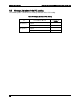
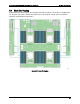
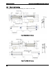
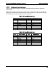
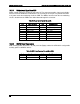

Table Of Contents
- 1. Introduction
- 2. Product Family Overview
- 3. Power Subsystem
- 3.1 Mechanical Overview
- 3.2 Power Connectors
- 3.3 Power Supply Module Efficiency
- 3.4 AC and DC Power Cord Specification Requirements
- 3.5 AC Input Specifications
- 3.5.1 Power Factor
- 3.5.2 AC Input Voltage Specification
- 3.5.3 AC Line Isolation Requirements
- 3.5.4 AC Line Dropout/Holdup
- 3.5.5 AC Line Fuse
- 3.5.6 AC Inrush
- 3.5.7 AC Line Transient Specification
- 3.5.8 Susceptibility Requirements
- 3.5.9 Electrostatic Discharge Susceptibility
- 3.5.10 Fast Transient/Burst
- 3.5.11 Radiated Immunity
- 3.5.12 Surge Immunity
- 3.5.13 Power Recovery
- 3.5.14 Voltage Interruptions
- 3.5.15 Protection Circuits
- 3.5.16 Over-current Protection (OCP)
- 3.5.17 Over-voltage Protection (OVP)
- 3.5.18 Over-temperature Protection (OTP)
- 3.6 1600W DC Power Supply Support
- 3.6.1 Power Supply Module Efficiency
- 3.6.2 DC Inlet Connector
- 3.6.3 DC Input Voltage Specification
- 3.6.4 DC Holdup/Dropout Time
- 3.6.5 DC Line Fuse
- 3.6.6 DC Inrush
- 3.6.7 DC Line Surge Voltages (Line Transients)
- 3.6.8 Residual Voltage Immunity in Standby Mode
- 3.6.9 Protection Circuits
- 3.6.10 Over Temperature Protection (OTP)
- 3.7 Cold Redundancy Support
- 3.8 Closed Loop System Throttling (CLST)
- 3.9 Smart Ride Through (SmaRT)
- 3.10 Power Supply Status LED
- 4. Thermal Management
- 5. System Storage and Peripheral Drive Bays Overview
- 6. Storage Controller Options Overview
- 7. Front Control Panel and I/O Panel Overview
- 8. Intel® Local Control Panel
- 9. PCI Riser Card Support
- 10. Additonal System Boards
- 11. Front Panel
- 12. IO Module Support
- 13. Intel® Intelligent Power Node Manager (NM)
- Appendix A: Integration and Usage Tip
- Appendix B: POST Code Diagnostic LED Decoder
- Appendix C: POST Code Errors
- Glossary
- Reference Documents
Additonal System Boards Intel® Server System R2000LH2/T2 Product Family TPS
Revision 1.0
86
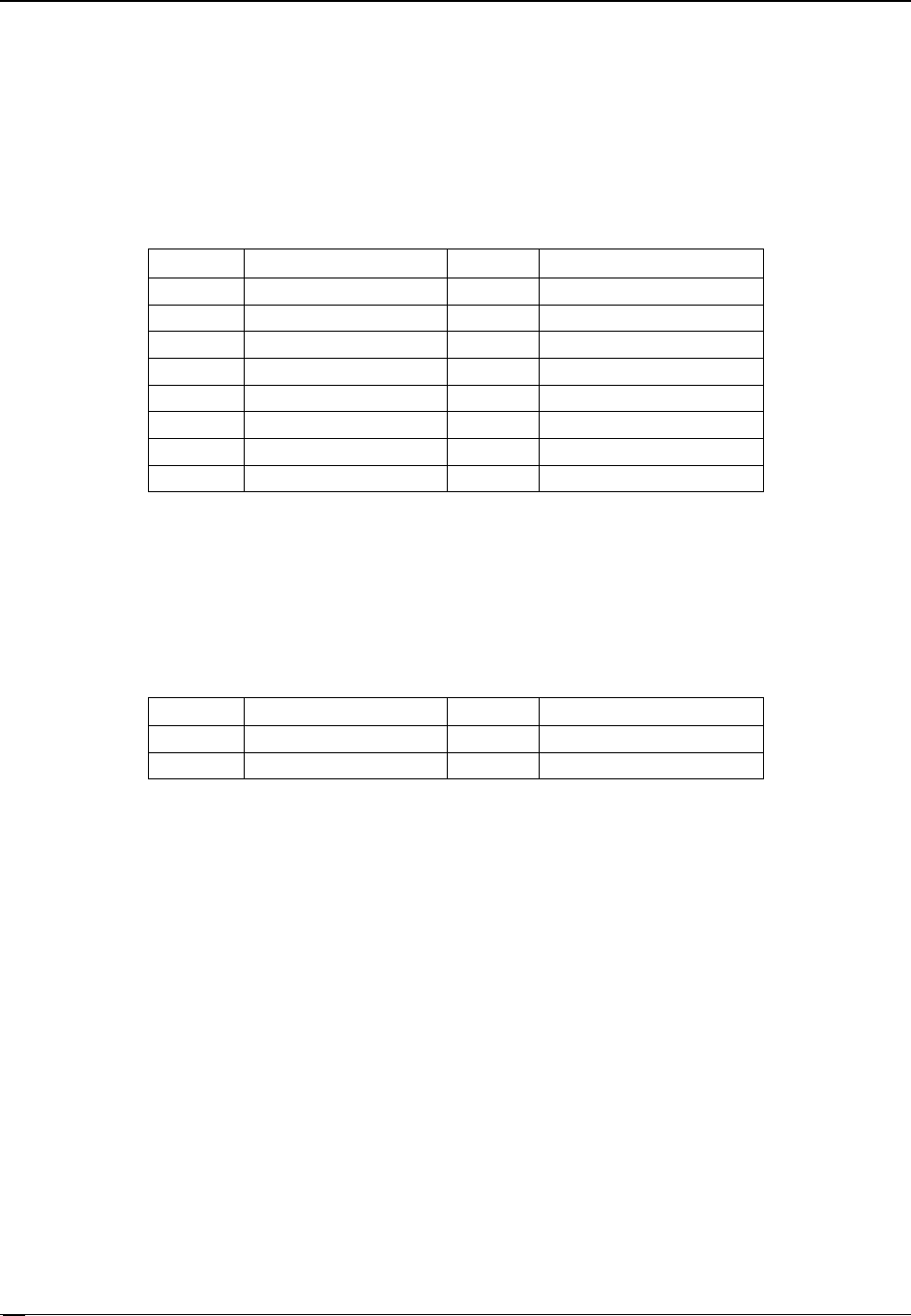
10.5.4
Motherboard Signal from PDB
Power control signals are routed via connector J5. The connector provides signal and 12Vstby
interface from the PDB to the motherboard. The 3.3Vstby and 3.3V pins are provided to allow
3.3V power to the fan monitoring circuit the PDB. The SMBus interface from the fan monitoring
circuit is routed from the PDB to the motherboard through this connector.
Table 39. Power Control Signals Pin-out (J5)
Pin #
Signal Description
Pin #
Signal Description
1
P3V3_STBY
9
Return_Sense
2
P3V3
10
P12V_Remote_Sense
3
PMBUS_SCL
11
P12V_STBY
4
PMBUS_SDA
12
P12V_STBY
5
PSON#
13
P12V_STBY
6
PWOK
14
P12V_STBY
7
SMBAlert#
15
FAN_SCL
8
Reserved
16
FAN_SDA
10.5.5
GPGPU Power Connectors
PDB auxiliary power connectors, J9 (Left) and J10 (Right), labeled for GFX add-in card, provide
auxiliary power to GPGPU devices.
Table 40. GPGPU Aux Connector Pin-out (J9 and J10)
Pin #
Signal Description
Pin #
Signal Description
1
GROUND
13
P12V1/2
2
GROUND
14
P12V1/2