
Technical Product Specification


Connector/Header Locations and Pin-out Intel® Server Board S1600JP TPS
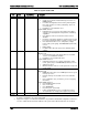
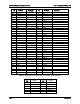
Side
Even
Pin Name
Side
Odd
Pin Name
16
PETxN14
15
PERxP14
14
GND
13
PERxN14
12
PETxP15
11
GND
10
PETxN15
9
PERxP15
8
GND
7
PERxN15
6
SMBUS_R4
CLK
5
GND
4
Spare
3
SMBUS_R4
DAT
2
Spare
1
Riser ID
Notes: There are 2 PCIe clock references from the riser slot: REFCLK1 and REFCLK2. If the riser is
designed as 1 x16 PCIe, BIOS will only enable REFCLK1 and disable REFCLK2. If the riser is split to 2
x8 PCIe, both REFCLK1 and REFCLK2 will be enabled for PCIe lane 0~7 and PCIe lane 8~15
respectively.
7.3.2
VGA Connector
The following table details the pin-out definition of the external VGA connector (J5A1) and so on.
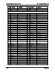
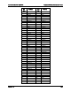
Table 65. VGA External Video Connector Pin-Out (J5A1)
Pin
Signal Name
Description
1
CRT_RED
Red (analog color signal R)
2
CRT_GREEN
Green (analog color signal G)
3
CRT_BLUE
Blue (analog color signal B)
4
NC
No connection
5
GND
Ground
6
GND
Ground
7
GND
Ground
8
GND
Ground
9
NC
No connection
10
GND
Ground
11
NC
No connection
12
CRT_DDCDATA
DDCDAT
13
CRT_HSYNC
HSYNC (horizontal sync)
14
CRT_VSYNC
VSYNC (vertical sync)
15
CRT_DDCCLK
DDCCLK
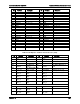
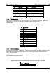
7.3.3
Internal Video for the front video
The following table details the pin-out of the internal video for front connector (J6A1) found on
the back edge of the server board.
Table 66. Internal Video Connector Pin-Out (J6A1)
Pin
Signal Name
Pin
Signal Name
1
Red
2
R_RTN (Red Return)
164 Revision 1.9