
User manual
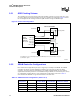


Table Of Contents
- Intel® IXP2800 Network Processor
- Copyright
- Contents
- Introduction 1
- Technical Description 2
- 2.1 Overview
- 2.2 Intel XScale® Core Microarchitecture
- 2.3 Microengines
- 2.4 DRAM
- 2.5 SRAM
- 2.6 Scratchpad Memory
- 2.7 Media and Switch Fabric Interface
- 2.8 Hash Unit
- 2.9 PCI Controller
- 2.10 Control and Status Register Access Proxy
- 2.11 Intel XScale® Core Peripherals
- 2.12 I/O Latency
- 2.13 Performance Monitor
- Intel XScale® Core 3
- 3.1 Introduction
- 3.2 Features
- 3.3 Memory Management
- 3.4 Instruction Cache
- 3.5 Branch Target Buffer (BTB)
- 3.6 Data Cache
- 3.6.1 Overviews
- 3.6.2 Data Cache and Mini-Data Cache Operation
- 3.6.3 Data Cache and Mini-Data Cache Control
- 3.6.4 Reconfiguring the Data Cache as Data RAM
- 3.6.5 Write Buffer/Fill Buffer Operation and Control
- 3.7 Configuration
- 3.8 Performance Monitoring
- 3.9 Performance Considerations
- 3.9.1 Interrupt Latency
- 3.9.2 Branch Prediction
- 3.9.3 Addressing Modes
- 3.9.4 Instruction Latencies
- 3.9.4.1 Performance Terms
- 3.9.4.2 Branch Instruction Timings
- 3.9.4.3 Data Processing Instruction Timings
- 3.9.4.4 Multiply Instruction Timings
- 3.9.4.5 Saturated Arithmetic Instructions
- 3.9.4.6 Status Register Access Instructions
- 3.9.4.7 Load/Store Instructions
- 3.9.4.8 Semaphore Instructions
- 3.9.4.9 Coprocessor Instructions
- 3.9.4.10 Miscellaneous Instruction Timing
- 3.9.4.11 Thumb Instructions
- 3.10 Test Features
- 3.11 Intel XScale® Core Gasket Unit
- 3.12 Intel XScale® Core Peripheral Interface
- 3.12.1 XPI Overview
- 3.12.2 UART Overview
- 3.12.3 UART Operation
- 3.12.4 Baud Rate Generator
- 3.12.5 General Purpose I/O (GPIO)
- 3.12.6 Timers
- 3.12.7 Slowport Unit
- Microengines 4
- DRAM 5
- SRAM Interface 6
- SHaC - Unit Expansion 7
- Media and Switch Fabric Interface 8
- 8.1 Overview
- 8.2 Receive
- 8.3 Transmit
- 8.4 RBUF and TBUF Summary
- 8.5 CSIX Flow Control Interface
- 8.6 Deskew and Training
- 8.7 CSIX Startup Sequence
- 8.8 Interface to Command and Push and Pull Buses
- 8.9 Receiver and Transmitter Interoperation with Framers and Switch Fabrics
- 8.9.1 Receiver and Transmitter Configurations
- 8.9.2 System Configurations
- 8.9.2.1 Framer, Single Network Processor Ingress and Egress, and Fabric Interface Chip
- 8.9.2.2 Framer, Dual Network Processor Ingress, Single Network Processor Egress, and Fabric Interface Chip
- 8.9.2.3 Framer, Single Network Processor Ingress and Egress, and CSIX-L1 Chips for Translation and Fabric Interface
- 8.9.2.4 CPU Complex, Network Processor, and Fabric Interface Chip
- 8.9.2.5 Framer, Single Network Processor, Co-Processor, and Fabric Interface Chip
- 8.9.3 SPI-4.2 Support
- 8.9.4 CSIX-L1 Protocol Support
- 8.9.5 Dual Protocol (SPI and CSIX-L1) Support
- 8.9.6 Transmit State Machine
- 8.9.7 Dynamic De-Skew
- 8.9.8 Summary of Receiver and Transmitter Signals
- PCI Unit 9
- 9.1 Overview
- 9.2 PCI Pin Protocol Interface Block
- 9.2.1 PCI Commands
- 9.2.2 IXP2800 Network Processor Initialization
- 9.2.3 PCI Type 0 Configuration Cycles
- 9.2.4 PCI 64-Bit Bus Extension
- 9.2.5 PCI Target Cycles
- 9.2.6 PCI Initiator Transactions
- 9.2.7 PCI Fast Back-to-Back Cycles
- 9.2.8 PCI Retry
- 9.2.9 PCI Disconnect
- 9.2.10 PCI Built-In System Test
- 9.2.11 PCI Central Functions
- 9.3 Slave Interface Block
- 9.4 Master Interface Block
- 9.5 PCI Unit Error Behavior
- 9.5.1 PCI Target Error Behavior
- 9.5.1.1 Target Access Has an Address Parity Error
- 9.5.1.2 Initiator Asserts PCI_PERR_L in Response to One of Our Data Phases
- 9.5.1.3 Discard Timer Expires on a Target Read
- 9.5.1.4 Target Access to the PCI_CSR_BAR Space Has Illegal Byte Enables
- 9.5.1.5 Target Write Access Receives Bad Parity PCI_PAR with the Data
- 9.5.1.6 SRAM Responds with a Memory Error on One or More Data Phases on a Target Read
- 9.5.1.7 DRAM Responds with a Memory Error on One or More Data Phases on a Target Read
- 9.5.2 As a PCI Initiator During a DMA Transfer
- 9.5.2.1 DMA Read from DRAM (Memory-to-PCI Transaction) Gets a Memory Error
- 9.5.2.2 DMA Read from SRAM (Descriptor Read) Gets a Memory Error
- 9.5.2.3 DMA from DRAM Transfer (Write to PCI) Receives PCI_PERR_L on PCI Bus
- 9.5.2.4 DMA To DRAM (Read from PCI) Has Bad Data Parity
- 9.5.2.5 DMA Transfer Experiences a Master Abort (Time-Out) on PCI
- 9.5.2.6 DMA Transfer Receives a Target Abort Response During a Data Phase
- 9.5.2.7 DMA Descriptor Has a 0x0 Word Count (Not an Error)
- 9.5.3 As a PCI Initiator During a Direct Access from the Intel XScale® Core or Microengine
- 9.5.3.1 Master Transfer Experiences a Master Abort (Time-Out) on PCI
- 9.5.3.2 Master Transfer Receives a Target Abort Response During a Data Phase
- 9.5.3.3 Master from the Intel XScale® Core or Microengine Transfer (Write to PCI) Receives PCI_PERR_L on PCI Bus
- 9.5.3.4 Master Read from PCI (Read from PCI) Has Bad Data Parity
- 9.5.3.5 Master Transfer Receives PCI_SERR_L from the PCI Bus
- 9.5.3.6 Intel XScale® Core Microengine Requests Direct Transfer when the PCI Bus is in Reset
- 9.5.1 PCI Target Error Behavior
- 9.6 PCI Data Byte Lane Alignment
- Clocks and Reset 10
- 10.1 Clocks
- 10.2 Synchronization Between Frequency Domains
- 10.3 Reset
- 10.4 Boot Mode
- 10.5 Initialization
- Performance Monitor Unit 11
- 11.1 Introduction
- 11.2 Interface and CSR Description
- 11.3 Performance Measurements
- 11.4 Events Monitored in Hardware
- 11.4.1 Queue Statistics Events
- 11.4.2 Count Events
- 11.4.3 Design Block Select Definitions
- 11.4.4 Null Event
- 11.4.5 Threshold Events
- 11.4.6 External Input Events
- 11.4.6.1 XPI Events Target ID(000001) / Design Block #(0100)
- 11.4.6.2 SHaC Events Target ID(000010) / Design Block #(0101)
- 11.4.6.3 IXP2800 Network Processor MSF Events Target ID(000011) / Design Block #(0110)
- 11.4.6.4 Intel XScale® Core Events Target ID(000100) / Design Block #(0111)
- 11.4.6.5 PCI Events Target ID(000101) / Design Block #(1000)
- 11.4.6.6 ME00 Events Target ID(100000) / Design Block #(1001)
- 11.4.6.7 ME01 Events Target ID(100001) / Design Block #(1001)
- 11.4.6.8 ME02 Events Target ID(100010) / Design Block #(1001)
- 11.4.6.9 ME03 Events Target ID(100011) / Design Block #(1001)
- 11.4.6.10 ME04 Events Target ID(100100) / Design Block #(1001)
- 11.4.6.11 ME05 Events Target ID(100101) / Design Block #(1001)
- 11.4.6.12 ME06 Events Target ID(100110) / Design Block #(1001)
- 11.4.6.13 ME07 Events Target ID(100111) / Design Block #(1001)
- 11.4.6.14 ME10 Events Target ID(110000) / Design Block #(1010)
- 11.4.6.15 ME11 Events Target ID(110001) / Design Block #(1010)
- 11.4.6.16 ME12 Events Target ID(110010) / Design Block #(1010)
- 11.4.6.17 ME13 Events Target ID(110011) / Design Block #(1010)
- 11.4.6.18 ME14 Events Target ID(110100) / Design Block #(1010)
- 11.4.6.19 ME15 Events Target ID(110101) / Design Block #(1010)
- 11.4.6.20 ME16 Events Target ID(100110) / Design Block #(1010)
- 11.4.6.21 ME17 Events Target ID(110111) / Design Block #(1010)
- 11.4.6.22 SRAM DP1 Events Target ID(001001) / Design Block #(0010)
- 11.4.6.23 SRAM DP0 Events Target ID(001010) / Design Block #(0010)
- 11.4.6.24 SRAM CH3 Events Target ID(001011) / Design Block #(0010)
- 11.4.6.25 SRAM CH2 Events Target ID(001100) / Design Block #(0010)
- 11.4.6.26 SRAM CH1 Events Target ID(001101) / Design Block #(0010)
- 11.4.6.27 SRAM CH0 Events Target ID(001110) / Design Block #(0010)
- 11.4.6.28 DRAM DPLA Events Target ID(010010) / Design Block #(0011)
- 11.4.6.29 DRAM DPSA Events Target ID(010011) / Design Block #(0011)
- 11.4.6.30 IXP2800 Network Processor DRAM CH2 Events Target ID(010100) / Design Block #(0011)
- 11.4.6.31 IXP2800 Network Processor DRAM CH1 Events Target ID(010101) / Design Block #(0011)
- 11.4.6.32 IXP2800 Network Processor DRAM CH0 Events Target ID(010110) / Design Block #(0011)

56 Hardware Reference Manual
Intel
®
IXP2800 Network Processor
Technical Description
2.5.5.2 Microengine Software Restrictions to Maintain Ordering
It is the Microengine programmer’s job to ensure order where the program flow finds order to be
necessary and where the architecture does not guarantee that order. The signaling mechanism can
be used to do this. For example, say that microcode needs to update several locations in a table. A
location in SRAM is used to “lock” access to the table. Example 13 is the code for the table update.
Other rules:
• All accesses to atomic variables should be via read-modify-write instructions.
• If the flow must know that a write is completed (actually in the SRAM itself), follow the write
with a read to the same address. The write is guaranteed to be complete when the read data has
been returned to the Microengine.
• With the exception of initialization, never do WRITE commands to the first three longwords
of a queue_descriptor data structure (these are the longwords that hold head, tail, and count,
etc.). All accesses to this data must be via the Q commands.
• To initialize the Q_array registers, perform a memory write of at least three longwords,
followed by a memory read to the same address (to guarantee that the write completed).
Then, for each entry in the Q_array, perform a read_q_descriptor_head followed by a
read_q_descriptor_other using the address of the same three longwords.
2.6 Scratchpad Memory
The IXP2800 Network Processor contains a 16 Kbytes of Scratchpad Memory, organized as 4K
32-bit words, that is accessible by Microengines and the Intel XScale
®
core. The Scratchpad
Memory provides the following operations:
• Normal reads and writes. 1–16 32-bit words can be read/written with a single Microengine
instruction. Note that Scratchpad is not byte-writable (each write must write all four bytes).
• Atomic read-modify-write operations, bit-set, bit-clear, increment, decrement, add, subtract,
and swap. The RMW operations can also optionally return the pre-modified data.
• Sixteen Hardware Assisted Rings for interprocess communication. (A ring is a FIFO that uses
a head and tail pointer to store/read information in Scratchpad memory.)
Scratchpad Memory is provided as a third memory resource (in addition to SRAM and DRAM)
that is shared by the Microengines and the Intel XScale
®
core. The Microengines and the Intel
XScale
®
core can distribute memory accesses between these three types of memory resources to
provide a greater number of memory accesses occurring in parallel.
Example 13. Table Update Code
IMMED [$xfer0, 1]
SRAM [write, $xfer0, flag_address, 0, 1], ctx_swap [SIG_DONE_2]
; At this point, the write to flag_address has passed the point of coherency. Do
the table updates.
SRAM [write, $xfer1, table_base, offset1, 2] , sig_done [SIG_DONE_3]
SRAM [write, $xfer3, table_base, offset2, 2] , sig_done [SIG_DONE_4]
CTX_ARB [SIG_DONE_3, SIG_DONE_4]
; At this point, the table writes have passed the point of coherency. Clear the
flag to allow access by other threads.
IMMED [$xfer0, 0]
SRAM [write, $xfer0, flag_address, 0, 1, ctx_swap [SIG_DONE_2]