
User manual

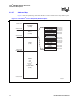
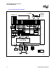
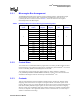
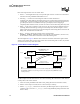

Table Of Contents
- Intel® IXP2800 Network Processor
- Copyright
- Contents
- Introduction 1
- Technical Description 2
- 2.1 Overview
- 2.2 Intel XScale® Core Microarchitecture
- 2.3 Microengines
- 2.4 DRAM
- 2.5 SRAM
- 2.6 Scratchpad Memory
- 2.7 Media and Switch Fabric Interface
- 2.8 Hash Unit
- 2.9 PCI Controller
- 2.10 Control and Status Register Access Proxy
- 2.11 Intel XScale® Core Peripherals
- 2.12 I/O Latency
- 2.13 Performance Monitor
- Intel XScale® Core 3
- 3.1 Introduction
- 3.2 Features
- 3.3 Memory Management
- 3.4 Instruction Cache
- 3.5 Branch Target Buffer (BTB)
- 3.6 Data Cache
- 3.6.1 Overviews
- 3.6.2 Data Cache and Mini-Data Cache Operation
- 3.6.3 Data Cache and Mini-Data Cache Control
- 3.6.4 Reconfiguring the Data Cache as Data RAM
- 3.6.5 Write Buffer/Fill Buffer Operation and Control
- 3.7 Configuration
- 3.8 Performance Monitoring
- 3.9 Performance Considerations
- 3.9.1 Interrupt Latency
- 3.9.2 Branch Prediction
- 3.9.3 Addressing Modes
- 3.9.4 Instruction Latencies
- 3.9.4.1 Performance Terms
- 3.9.4.2 Branch Instruction Timings
- 3.9.4.3 Data Processing Instruction Timings
- 3.9.4.4 Multiply Instruction Timings
- 3.9.4.5 Saturated Arithmetic Instructions
- 3.9.4.6 Status Register Access Instructions
- 3.9.4.7 Load/Store Instructions
- 3.9.4.8 Semaphore Instructions
- 3.9.4.9 Coprocessor Instructions
- 3.9.4.10 Miscellaneous Instruction Timing
- 3.9.4.11 Thumb Instructions
- 3.10 Test Features
- 3.11 Intel XScale® Core Gasket Unit
- 3.12 Intel XScale® Core Peripheral Interface
- 3.12.1 XPI Overview
- 3.12.2 UART Overview
- 3.12.3 UART Operation
- 3.12.4 Baud Rate Generator
- 3.12.5 General Purpose I/O (GPIO)
- 3.12.6 Timers
- 3.12.7 Slowport Unit
- Microengines 4
- DRAM 5
- SRAM Interface 6
- SHaC - Unit Expansion 7
- Media and Switch Fabric Interface 8
- 8.1 Overview
- 8.2 Receive
- 8.3 Transmit
- 8.4 RBUF and TBUF Summary
- 8.5 CSIX Flow Control Interface
- 8.6 Deskew and Training
- 8.7 CSIX Startup Sequence
- 8.8 Interface to Command and Push and Pull Buses
- 8.9 Receiver and Transmitter Interoperation with Framers and Switch Fabrics
- 8.9.1 Receiver and Transmitter Configurations
- 8.9.2 System Configurations
- 8.9.2.1 Framer, Single Network Processor Ingress and Egress, and Fabric Interface Chip
- 8.9.2.2 Framer, Dual Network Processor Ingress, Single Network Processor Egress, and Fabric Interface Chip
- 8.9.2.3 Framer, Single Network Processor Ingress and Egress, and CSIX-L1 Chips for Translation and Fabric Interface
- 8.9.2.4 CPU Complex, Network Processor, and Fabric Interface Chip
- 8.9.2.5 Framer, Single Network Processor, Co-Processor, and Fabric Interface Chip
- 8.9.3 SPI-4.2 Support
- 8.9.4 CSIX-L1 Protocol Support
- 8.9.5 Dual Protocol (SPI and CSIX-L1) Support
- 8.9.6 Transmit State Machine
- 8.9.7 Dynamic De-Skew
- 8.9.8 Summary of Receiver and Transmitter Signals
- PCI Unit 9
- 9.1 Overview
- 9.2 PCI Pin Protocol Interface Block
- 9.2.1 PCI Commands
- 9.2.2 IXP2800 Network Processor Initialization
- 9.2.3 PCI Type 0 Configuration Cycles
- 9.2.4 PCI 64-Bit Bus Extension
- 9.2.5 PCI Target Cycles
- 9.2.6 PCI Initiator Transactions
- 9.2.7 PCI Fast Back-to-Back Cycles
- 9.2.8 PCI Retry
- 9.2.9 PCI Disconnect
- 9.2.10 PCI Built-In System Test
- 9.2.11 PCI Central Functions
- 9.3 Slave Interface Block
- 9.4 Master Interface Block
- 9.5 PCI Unit Error Behavior
- 9.5.1 PCI Target Error Behavior
- 9.5.1.1 Target Access Has an Address Parity Error
- 9.5.1.2 Initiator Asserts PCI_PERR_L in Response to One of Our Data Phases
- 9.5.1.3 Discard Timer Expires on a Target Read
- 9.5.1.4 Target Access to the PCI_CSR_BAR Space Has Illegal Byte Enables
- 9.5.1.5 Target Write Access Receives Bad Parity PCI_PAR with the Data
- 9.5.1.6 SRAM Responds with a Memory Error on One or More Data Phases on a Target Read
- 9.5.1.7 DRAM Responds with a Memory Error on One or More Data Phases on a Target Read
- 9.5.2 As a PCI Initiator During a DMA Transfer
- 9.5.2.1 DMA Read from DRAM (Memory-to-PCI Transaction) Gets a Memory Error
- 9.5.2.2 DMA Read from SRAM (Descriptor Read) Gets a Memory Error
- 9.5.2.3 DMA from DRAM Transfer (Write to PCI) Receives PCI_PERR_L on PCI Bus
- 9.5.2.4 DMA To DRAM (Read from PCI) Has Bad Data Parity
- 9.5.2.5 DMA Transfer Experiences a Master Abort (Time-Out) on PCI
- 9.5.2.6 DMA Transfer Receives a Target Abort Response During a Data Phase
- 9.5.2.7 DMA Descriptor Has a 0x0 Word Count (Not an Error)
- 9.5.3 As a PCI Initiator During a Direct Access from the Intel XScale® Core or Microengine
- 9.5.3.1 Master Transfer Experiences a Master Abort (Time-Out) on PCI
- 9.5.3.2 Master Transfer Receives a Target Abort Response During a Data Phase
- 9.5.3.3 Master from the Intel XScale® Core or Microengine Transfer (Write to PCI) Receives PCI_PERR_L on PCI Bus
- 9.5.3.4 Master Read from PCI (Read from PCI) Has Bad Data Parity
- 9.5.3.5 Master Transfer Receives PCI_SERR_L from the PCI Bus
- 9.5.3.6 Intel XScale® Core Microengine Requests Direct Transfer when the PCI Bus is in Reset
- 9.5.1 PCI Target Error Behavior
- 9.6 PCI Data Byte Lane Alignment
- Clocks and Reset 10
- 10.1 Clocks
- 10.2 Synchronization Between Frequency Domains
- 10.3 Reset
- 10.4 Boot Mode
- 10.5 Initialization
- Performance Monitor Unit 11
- 11.1 Introduction
- 11.2 Interface and CSR Description
- 11.3 Performance Measurements
- 11.4 Events Monitored in Hardware
- 11.4.1 Queue Statistics Events
- 11.4.2 Count Events
- 11.4.3 Design Block Select Definitions
- 11.4.4 Null Event
- 11.4.5 Threshold Events
- 11.4.6 External Input Events
- 11.4.6.1 XPI Events Target ID(000001) / Design Block #(0100)
- 11.4.6.2 SHaC Events Target ID(000010) / Design Block #(0101)
- 11.4.6.3 IXP2800 Network Processor MSF Events Target ID(000011) / Design Block #(0110)
- 11.4.6.4 Intel XScale® Core Events Target ID(000100) / Design Block #(0111)
- 11.4.6.5 PCI Events Target ID(000101) / Design Block #(1000)
- 11.4.6.6 ME00 Events Target ID(100000) / Design Block #(1001)
- 11.4.6.7 ME01 Events Target ID(100001) / Design Block #(1001)
- 11.4.6.8 ME02 Events Target ID(100010) / Design Block #(1001)
- 11.4.6.9 ME03 Events Target ID(100011) / Design Block #(1001)
- 11.4.6.10 ME04 Events Target ID(100100) / Design Block #(1001)
- 11.4.6.11 ME05 Events Target ID(100101) / Design Block #(1001)
- 11.4.6.12 ME06 Events Target ID(100110) / Design Block #(1001)
- 11.4.6.13 ME07 Events Target ID(100111) / Design Block #(1001)
- 11.4.6.14 ME10 Events Target ID(110000) / Design Block #(1010)
- 11.4.6.15 ME11 Events Target ID(110001) / Design Block #(1010)
- 11.4.6.16 ME12 Events Target ID(110010) / Design Block #(1010)
- 11.4.6.17 ME13 Events Target ID(110011) / Design Block #(1010)
- 11.4.6.18 ME14 Events Target ID(110100) / Design Block #(1010)
- 11.4.6.19 ME15 Events Target ID(110101) / Design Block #(1010)
- 11.4.6.20 ME16 Events Target ID(100110) / Design Block #(1010)
- 11.4.6.21 ME17 Events Target ID(110111) / Design Block #(1010)
- 11.4.6.22 SRAM DP1 Events Target ID(001001) / Design Block #(0010)
- 11.4.6.23 SRAM DP0 Events Target ID(001010) / Design Block #(0010)
- 11.4.6.24 SRAM CH3 Events Target ID(001011) / Design Block #(0010)
- 11.4.6.25 SRAM CH2 Events Target ID(001100) / Design Block #(0010)
- 11.4.6.26 SRAM CH1 Events Target ID(001101) / Design Block #(0010)
- 11.4.6.27 SRAM CH0 Events Target ID(001110) / Design Block #(0010)
- 11.4.6.28 DRAM DPLA Events Target ID(010010) / Design Block #(0011)
- 11.4.6.29 DRAM DPSA Events Target ID(010011) / Design Block #(0011)
- 11.4.6.30 IXP2800 Network Processor DRAM CH2 Events Target ID(010100) / Design Block #(0011)
- 11.4.6.31 IXP2800 Network Processor DRAM CH1 Events Target ID(010101) / Design Block #(0011)
- 11.4.6.32 IXP2800 Network Processor DRAM CH0 Events Target ID(010110) / Design Block #(0011)

Hardware Reference Manual 37
Intel
®
IXP2800 Network Processor
Technical Description
The Microengine provides the following functionality during the Idle state:
1. The Microengine continuously checks if a Context is in Ready state. If so, a new Context
begins to execute. If no Context is Ready, the Microengine remains in the Idle state.
2. Only the ALU instructions are supported. They are used for debug via special hardware
defined in number 3 below.
3. A write to the USTORE_ADDR Local CSR with the USTORE_ADDR[ECS] bit set, causing
the Microengine to repeatedly execute the instruction pointed by the address specified in the
USTORE_ADDR CSR. Only the ALU instructions are supported in this mode. Also, the result
of the execution is written to the ALU_OUT Local CSR rather than a destination register.
4. A write to the USTORE_ADDR Local CSR with the USTORE_ADDR[ECS] bit set, followed
by a write to the USTORE_DATA Local CSR loads an instruction into the Control Store. After
the Control Store is loaded, execution proceeds as described in number 3 above.
2.3.4 Datapath Registers
As shown in the block diagram in Figure 4, each Microengine contains four types of 32-bit
datapath registers:
1. 256 General Purpose registers
2. 512 Transfer registers
3. 128 Next Neighbor registers
4. 640 32-bit words of Local Memory
2.3.4.1 General-Purpose Registers (GPRs)
GPRs are used for general programming purposes. They are read and written exclusively under
program control. GPRs, when used as a source in an instruction, supply operands to the execution
datapath. When used as a destination in an instruction, they are written with the result of the
execution datapath. The specific GPRs selected are encoded in the instruction.
The GPRs are physically and logically contained in two banks, GPR A, and GPR B, defined in
Table 5.
2.3.4.2 Transfer Registers
Transfer (abbreviated as Xfer) registers are used for transferring data to and from the Microengine
and locations external to the Microengine, (for example DRAMs, SRAMs etc.). There are four
types of transfer registers.
• S_TRANSFER_IN
• S_TRANSFER_OUT
• D_TRANSFER_IN
• D_TRANSFER_OUT
TRANSFER_IN registers, when used as a source in an instruction, supply operands to the
execution datapath. The specific register selected is either encoded in the instruction, or selected
indirectly via T_INDEX. TRANSFER_IN registers are written by external units (A typical case is
when the external unit returns data in response to read instructions. However, there are other