
User manual
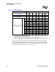
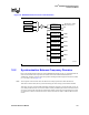
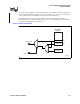


Table Of Contents
- Intel® IXP2800 Network Processor
- Copyright
- Contents
- Introduction 1
- Technical Description 2
- 2.1 Overview
- 2.2 Intel XScale® Core Microarchitecture
- 2.3 Microengines
- 2.4 DRAM
- 2.5 SRAM
- 2.6 Scratchpad Memory
- 2.7 Media and Switch Fabric Interface
- 2.8 Hash Unit
- 2.9 PCI Controller
- 2.10 Control and Status Register Access Proxy
- 2.11 Intel XScale® Core Peripherals
- 2.12 I/O Latency
- 2.13 Performance Monitor
- Intel XScale® Core 3
- 3.1 Introduction
- 3.2 Features
- 3.3 Memory Management
- 3.4 Instruction Cache
- 3.5 Branch Target Buffer (BTB)
- 3.6 Data Cache
- 3.6.1 Overviews
- 3.6.2 Data Cache and Mini-Data Cache Operation
- 3.6.3 Data Cache and Mini-Data Cache Control
- 3.6.4 Reconfiguring the Data Cache as Data RAM
- 3.6.5 Write Buffer/Fill Buffer Operation and Control
- 3.7 Configuration
- 3.8 Performance Monitoring
- 3.9 Performance Considerations
- 3.9.1 Interrupt Latency
- 3.9.2 Branch Prediction
- 3.9.3 Addressing Modes
- 3.9.4 Instruction Latencies
- 3.9.4.1 Performance Terms
- 3.9.4.2 Branch Instruction Timings
- 3.9.4.3 Data Processing Instruction Timings
- 3.9.4.4 Multiply Instruction Timings
- 3.9.4.5 Saturated Arithmetic Instructions
- 3.9.4.6 Status Register Access Instructions
- 3.9.4.7 Load/Store Instructions
- 3.9.4.8 Semaphore Instructions
- 3.9.4.9 Coprocessor Instructions
- 3.9.4.10 Miscellaneous Instruction Timing
- 3.9.4.11 Thumb Instructions
- 3.10 Test Features
- 3.11 Intel XScale® Core Gasket Unit
- 3.12 Intel XScale® Core Peripheral Interface
- 3.12.1 XPI Overview
- 3.12.2 UART Overview
- 3.12.3 UART Operation
- 3.12.4 Baud Rate Generator
- 3.12.5 General Purpose I/O (GPIO)
- 3.12.6 Timers
- 3.12.7 Slowport Unit
- Microengines 4
- DRAM 5
- SRAM Interface 6
- SHaC - Unit Expansion 7
- Media and Switch Fabric Interface 8
- 8.1 Overview
- 8.2 Receive
- 8.3 Transmit
- 8.4 RBUF and TBUF Summary
- 8.5 CSIX Flow Control Interface
- 8.6 Deskew and Training
- 8.7 CSIX Startup Sequence
- 8.8 Interface to Command and Push and Pull Buses
- 8.9 Receiver and Transmitter Interoperation with Framers and Switch Fabrics
- 8.9.1 Receiver and Transmitter Configurations
- 8.9.2 System Configurations
- 8.9.2.1 Framer, Single Network Processor Ingress and Egress, and Fabric Interface Chip
- 8.9.2.2 Framer, Dual Network Processor Ingress, Single Network Processor Egress, and Fabric Interface Chip
- 8.9.2.3 Framer, Single Network Processor Ingress and Egress, and CSIX-L1 Chips for Translation and Fabric Interface
- 8.9.2.4 CPU Complex, Network Processor, and Fabric Interface Chip
- 8.9.2.5 Framer, Single Network Processor, Co-Processor, and Fabric Interface Chip
- 8.9.3 SPI-4.2 Support
- 8.9.4 CSIX-L1 Protocol Support
- 8.9.5 Dual Protocol (SPI and CSIX-L1) Support
- 8.9.6 Transmit State Machine
- 8.9.7 Dynamic De-Skew
- 8.9.8 Summary of Receiver and Transmitter Signals
- PCI Unit 9
- 9.1 Overview
- 9.2 PCI Pin Protocol Interface Block
- 9.2.1 PCI Commands
- 9.2.2 IXP2800 Network Processor Initialization
- 9.2.3 PCI Type 0 Configuration Cycles
- 9.2.4 PCI 64-Bit Bus Extension
- 9.2.5 PCI Target Cycles
- 9.2.6 PCI Initiator Transactions
- 9.2.7 PCI Fast Back-to-Back Cycles
- 9.2.8 PCI Retry
- 9.2.9 PCI Disconnect
- 9.2.10 PCI Built-In System Test
- 9.2.11 PCI Central Functions
- 9.3 Slave Interface Block
- 9.4 Master Interface Block
- 9.5 PCI Unit Error Behavior
- 9.5.1 PCI Target Error Behavior
- 9.5.1.1 Target Access Has an Address Parity Error
- 9.5.1.2 Initiator Asserts PCI_PERR_L in Response to One of Our Data Phases
- 9.5.1.3 Discard Timer Expires on a Target Read
- 9.5.1.4 Target Access to the PCI_CSR_BAR Space Has Illegal Byte Enables
- 9.5.1.5 Target Write Access Receives Bad Parity PCI_PAR with the Data
- 9.5.1.6 SRAM Responds with a Memory Error on One or More Data Phases on a Target Read
- 9.5.1.7 DRAM Responds with a Memory Error on One or More Data Phases on a Target Read
- 9.5.2 As a PCI Initiator During a DMA Transfer
- 9.5.2.1 DMA Read from DRAM (Memory-to-PCI Transaction) Gets a Memory Error
- 9.5.2.2 DMA Read from SRAM (Descriptor Read) Gets a Memory Error
- 9.5.2.3 DMA from DRAM Transfer (Write to PCI) Receives PCI_PERR_L on PCI Bus
- 9.5.2.4 DMA To DRAM (Read from PCI) Has Bad Data Parity
- 9.5.2.5 DMA Transfer Experiences a Master Abort (Time-Out) on PCI
- 9.5.2.6 DMA Transfer Receives a Target Abort Response During a Data Phase
- 9.5.2.7 DMA Descriptor Has a 0x0 Word Count (Not an Error)
- 9.5.3 As a PCI Initiator During a Direct Access from the Intel XScale® Core or Microengine
- 9.5.3.1 Master Transfer Experiences a Master Abort (Time-Out) on PCI
- 9.5.3.2 Master Transfer Receives a Target Abort Response During a Data Phase
- 9.5.3.3 Master from the Intel XScale® Core or Microengine Transfer (Write to PCI) Receives PCI_PERR_L on PCI Bus
- 9.5.3.4 Master Read from PCI (Read from PCI) Has Bad Data Parity
- 9.5.3.5 Master Transfer Receives PCI_SERR_L from the PCI Bus
- 9.5.3.6 Intel XScale® Core Microengine Requests Direct Transfer when the PCI Bus is in Reset
- 9.5.1 PCI Target Error Behavior
- 9.6 PCI Data Byte Lane Alignment
- Clocks and Reset 10
- 10.1 Clocks
- 10.2 Synchronization Between Frequency Domains
- 10.3 Reset
- 10.4 Boot Mode
- 10.5 Initialization
- Performance Monitor Unit 11
- 11.1 Introduction
- 11.2 Interface and CSR Description
- 11.3 Performance Measurements
- 11.4 Events Monitored in Hardware
- 11.4.1 Queue Statistics Events
- 11.4.2 Count Events
- 11.4.3 Design Block Select Definitions
- 11.4.4 Null Event
- 11.4.5 Threshold Events
- 11.4.6 External Input Events
- 11.4.6.1 XPI Events Target ID(000001) / Design Block #(0100)
- 11.4.6.2 SHaC Events Target ID(000010) / Design Block #(0101)
- 11.4.6.3 IXP2800 Network Processor MSF Events Target ID(000011) / Design Block #(0110)
- 11.4.6.4 Intel XScale® Core Events Target ID(000100) / Design Block #(0111)
- 11.4.6.5 PCI Events Target ID(000101) / Design Block #(1000)
- 11.4.6.6 ME00 Events Target ID(100000) / Design Block #(1001)
- 11.4.6.7 ME01 Events Target ID(100001) / Design Block #(1001)
- 11.4.6.8 ME02 Events Target ID(100010) / Design Block #(1001)
- 11.4.6.9 ME03 Events Target ID(100011) / Design Block #(1001)
- 11.4.6.10 ME04 Events Target ID(100100) / Design Block #(1001)
- 11.4.6.11 ME05 Events Target ID(100101) / Design Block #(1001)
- 11.4.6.12 ME06 Events Target ID(100110) / Design Block #(1001)
- 11.4.6.13 ME07 Events Target ID(100111) / Design Block #(1001)
- 11.4.6.14 ME10 Events Target ID(110000) / Design Block #(1010)
- 11.4.6.15 ME11 Events Target ID(110001) / Design Block #(1010)
- 11.4.6.16 ME12 Events Target ID(110010) / Design Block #(1010)
- 11.4.6.17 ME13 Events Target ID(110011) / Design Block #(1010)
- 11.4.6.18 ME14 Events Target ID(110100) / Design Block #(1010)
- 11.4.6.19 ME15 Events Target ID(110101) / Design Block #(1010)
- 11.4.6.20 ME16 Events Target ID(100110) / Design Block #(1010)
- 11.4.6.21 ME17 Events Target ID(110111) / Design Block #(1010)
- 11.4.6.22 SRAM DP1 Events Target ID(001001) / Design Block #(0010)
- 11.4.6.23 SRAM DP0 Events Target ID(001010) / Design Block #(0010)
- 11.4.6.24 SRAM CH3 Events Target ID(001011) / Design Block #(0010)
- 11.4.6.25 SRAM CH2 Events Target ID(001100) / Design Block #(0010)
- 11.4.6.26 SRAM CH1 Events Target ID(001101) / Design Block #(0010)
- 11.4.6.27 SRAM CH0 Events Target ID(001110) / Design Block #(0010)
- 11.4.6.28 DRAM DPLA Events Target ID(010010) / Design Block #(0011)
- 11.4.6.29 DRAM DPSA Events Target ID(010011) / Design Block #(0011)
- 11.4.6.30 IXP2800 Network Processor DRAM CH2 Events Target ID(010100) / Design Block #(0011)
- 11.4.6.31 IXP2800 Network Processor DRAM CH1 Events Target ID(010101) / Design Block #(0011)
- 11.4.6.32 IXP2800 Network Processor DRAM CH0 Events Target ID(010110) / Design Block #(0011)
Hardware Reference Manual 361
Intel
®
IXP2800 Network Processor
Clocks and Reset
The fast frequency on the IXP2800 Network Processor is generated by an on-chip PLL that
multiplies a reference frequency provided by an on-board LVDS oscillator (frequency 100 MHz)
by a selectable multiplier. The multiplier is selected by using external strap pins SP_AD[5:0] and
can be viewed by software via the STRAP_OPTIONS[CFG_PLL_MULT] CAP CSR register bits.
The multiplier range is even multiples between 16 and 48, so the PLL can generate a 1.6 GHz to
4.8 GHz clock (with a 100-Mhz reference frequency).
The PLL output frequency is divided by 2 to get the Microengine clock and by 4 to get the Intel
XScale
®
core and the internal Command/Push/Pull bus frequency. An additional division (after the
divide by 2) is used to generate the clock frequencies for the other internal units. The divisors are
programmable via the CLOCK_CONTROL CSR. APB divisor specified in the
CLOCK_CONTROL CSR clock is scaled by 4 (i.e., a value of 2 in the CSR selects a divisor of 8).
Table 148 shows the frequencies that are available based on a 100-Mhz oscillator and various
values of PLL multipliers, for the supported divisor values of 3 to 15.
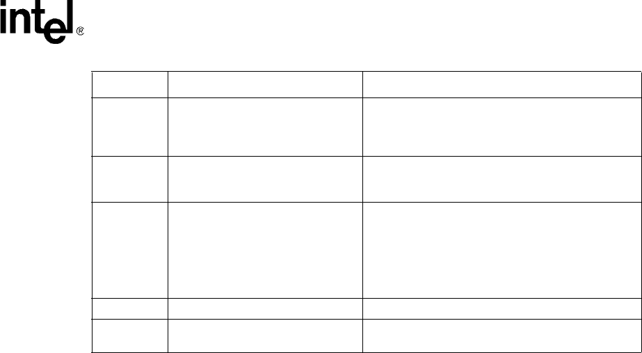
SRAM
SRAM pins and control logic (all of
the SRAM unit except Internal Bus
interface).
Divide of Microengine frequency. Each SRAM channel
has its own frequency selection. Clocks are driven by
the IXP2800 Network Processor to external SRAMs
and/or Coprocessors.
Scratch,
Hash, CSR
Scratch RAM, Hash Unit, CSR
access block
1/2 of Microengine frequency. Note that Slowport has
no clock. Timing for Slowport accesses is defined in
Slowport registers.
MSF
Receive and Transmit pins and
control logic.
The transmit clock for the Media and Switch interface
can be derived in two different ways.
• From TCLK input signal (supplied by PHY device).
• Divided from internal clock.
For details please refer to Chapter 8, “Media and
Switch Fabric Interface”.
APB APB logic Divide of Microengine frequency.
PCI PCI pins and control logic.
External reference. Either from Host system or on-
board oscillator.
Table 147. Clock Usage Summary (Sheet 2 of 2)
Unit Name Description Comment