
User manual


Table Of Contents
- Intel® IXP2800 Network Processor
- Copyright
- Contents
- Introduction 1
- Technical Description 2
- 2.1 Overview
- 2.2 Intel XScale® Core Microarchitecture
- 2.3 Microengines
- 2.4 DRAM
- 2.5 SRAM
- 2.6 Scratchpad Memory
- 2.7 Media and Switch Fabric Interface
- 2.8 Hash Unit
- 2.9 PCI Controller
- 2.10 Control and Status Register Access Proxy
- 2.11 Intel XScale® Core Peripherals
- 2.12 I/O Latency
- 2.13 Performance Monitor
- Intel XScale® Core 3
- 3.1 Introduction
- 3.2 Features
- 3.3 Memory Management
- 3.4 Instruction Cache
- 3.5 Branch Target Buffer (BTB)
- 3.6 Data Cache
- 3.6.1 Overviews
- 3.6.2 Data Cache and Mini-Data Cache Operation
- 3.6.3 Data Cache and Mini-Data Cache Control
- 3.6.4 Reconfiguring the Data Cache as Data RAM
- 3.6.5 Write Buffer/Fill Buffer Operation and Control
- 3.7 Configuration
- 3.8 Performance Monitoring
- 3.9 Performance Considerations
- 3.9.1 Interrupt Latency
- 3.9.2 Branch Prediction
- 3.9.3 Addressing Modes
- 3.9.4 Instruction Latencies
- 3.9.4.1 Performance Terms
- 3.9.4.2 Branch Instruction Timings
- 3.9.4.3 Data Processing Instruction Timings
- 3.9.4.4 Multiply Instruction Timings
- 3.9.4.5 Saturated Arithmetic Instructions
- 3.9.4.6 Status Register Access Instructions
- 3.9.4.7 Load/Store Instructions
- 3.9.4.8 Semaphore Instructions
- 3.9.4.9 Coprocessor Instructions
- 3.9.4.10 Miscellaneous Instruction Timing
- 3.9.4.11 Thumb Instructions
- 3.10 Test Features
- 3.11 Intel XScale® Core Gasket Unit
- 3.12 Intel XScale® Core Peripheral Interface
- 3.12.1 XPI Overview
- 3.12.2 UART Overview
- 3.12.3 UART Operation
- 3.12.4 Baud Rate Generator
- 3.12.5 General Purpose I/O (GPIO)
- 3.12.6 Timers
- 3.12.7 Slowport Unit
- Microengines 4
- DRAM 5
- SRAM Interface 6
- SHaC - Unit Expansion 7
- Media and Switch Fabric Interface 8
- 8.1 Overview
- 8.2 Receive
- 8.3 Transmit
- 8.4 RBUF and TBUF Summary
- 8.5 CSIX Flow Control Interface
- 8.6 Deskew and Training
- 8.7 CSIX Startup Sequence
- 8.8 Interface to Command and Push and Pull Buses
- 8.9 Receiver and Transmitter Interoperation with Framers and Switch Fabrics
- 8.9.1 Receiver and Transmitter Configurations
- 8.9.2 System Configurations
- 8.9.2.1 Framer, Single Network Processor Ingress and Egress, and Fabric Interface Chip
- 8.9.2.2 Framer, Dual Network Processor Ingress, Single Network Processor Egress, and Fabric Interface Chip
- 8.9.2.3 Framer, Single Network Processor Ingress and Egress, and CSIX-L1 Chips for Translation and Fabric Interface
- 8.9.2.4 CPU Complex, Network Processor, and Fabric Interface Chip
- 8.9.2.5 Framer, Single Network Processor, Co-Processor, and Fabric Interface Chip
- 8.9.3 SPI-4.2 Support
- 8.9.4 CSIX-L1 Protocol Support
- 8.9.5 Dual Protocol (SPI and CSIX-L1) Support
- 8.9.6 Transmit State Machine
- 8.9.7 Dynamic De-Skew
- 8.9.8 Summary of Receiver and Transmitter Signals
- PCI Unit 9
- 9.1 Overview
- 9.2 PCI Pin Protocol Interface Block
- 9.2.1 PCI Commands
- 9.2.2 IXP2800 Network Processor Initialization
- 9.2.3 PCI Type 0 Configuration Cycles
- 9.2.4 PCI 64-Bit Bus Extension
- 9.2.5 PCI Target Cycles
- 9.2.6 PCI Initiator Transactions
- 9.2.7 PCI Fast Back-to-Back Cycles
- 9.2.8 PCI Retry
- 9.2.9 PCI Disconnect
- 9.2.10 PCI Built-In System Test
- 9.2.11 PCI Central Functions
- 9.3 Slave Interface Block
- 9.4 Master Interface Block
- 9.5 PCI Unit Error Behavior
- 9.5.1 PCI Target Error Behavior
- 9.5.1.1 Target Access Has an Address Parity Error
- 9.5.1.2 Initiator Asserts PCI_PERR_L in Response to One of Our Data Phases
- 9.5.1.3 Discard Timer Expires on a Target Read
- 9.5.1.4 Target Access to the PCI_CSR_BAR Space Has Illegal Byte Enables
- 9.5.1.5 Target Write Access Receives Bad Parity PCI_PAR with the Data
- 9.5.1.6 SRAM Responds with a Memory Error on One or More Data Phases on a Target Read
- 9.5.1.7 DRAM Responds with a Memory Error on One or More Data Phases on a Target Read
- 9.5.2 As a PCI Initiator During a DMA Transfer
- 9.5.2.1 DMA Read from DRAM (Memory-to-PCI Transaction) Gets a Memory Error
- 9.5.2.2 DMA Read from SRAM (Descriptor Read) Gets a Memory Error
- 9.5.2.3 DMA from DRAM Transfer (Write to PCI) Receives PCI_PERR_L on PCI Bus
- 9.5.2.4 DMA To DRAM (Read from PCI) Has Bad Data Parity
- 9.5.2.5 DMA Transfer Experiences a Master Abort (Time-Out) on PCI
- 9.5.2.6 DMA Transfer Receives a Target Abort Response During a Data Phase
- 9.5.2.7 DMA Descriptor Has a 0x0 Word Count (Not an Error)
- 9.5.3 As a PCI Initiator During a Direct Access from the Intel XScale® Core or Microengine
- 9.5.3.1 Master Transfer Experiences a Master Abort (Time-Out) on PCI
- 9.5.3.2 Master Transfer Receives a Target Abort Response During a Data Phase
- 9.5.3.3 Master from the Intel XScale® Core or Microengine Transfer (Write to PCI) Receives PCI_PERR_L on PCI Bus
- 9.5.3.4 Master Read from PCI (Read from PCI) Has Bad Data Parity
- 9.5.3.5 Master Transfer Receives PCI_SERR_L from the PCI Bus
- 9.5.3.6 Intel XScale® Core Microengine Requests Direct Transfer when the PCI Bus is in Reset
- 9.5.1 PCI Target Error Behavior
- 9.6 PCI Data Byte Lane Alignment
- Clocks and Reset 10
- 10.1 Clocks
- 10.2 Synchronization Between Frequency Domains
- 10.3 Reset
- 10.4 Boot Mode
- 10.5 Initialization
- Performance Monitor Unit 11
- 11.1 Introduction
- 11.2 Interface and CSR Description
- 11.3 Performance Measurements
- 11.4 Events Monitored in Hardware
- 11.4.1 Queue Statistics Events
- 11.4.2 Count Events
- 11.4.3 Design Block Select Definitions
- 11.4.4 Null Event
- 11.4.5 Threshold Events
- 11.4.6 External Input Events
- 11.4.6.1 XPI Events Target ID(000001) / Design Block #(0100)
- 11.4.6.2 SHaC Events Target ID(000010) / Design Block #(0101)
- 11.4.6.3 IXP2800 Network Processor MSF Events Target ID(000011) / Design Block #(0110)
- 11.4.6.4 Intel XScale® Core Events Target ID(000100) / Design Block #(0111)
- 11.4.6.5 PCI Events Target ID(000101) / Design Block #(1000)
- 11.4.6.6 ME00 Events Target ID(100000) / Design Block #(1001)
- 11.4.6.7 ME01 Events Target ID(100001) / Design Block #(1001)
- 11.4.6.8 ME02 Events Target ID(100010) / Design Block #(1001)
- 11.4.6.9 ME03 Events Target ID(100011) / Design Block #(1001)
- 11.4.6.10 ME04 Events Target ID(100100) / Design Block #(1001)
- 11.4.6.11 ME05 Events Target ID(100101) / Design Block #(1001)
- 11.4.6.12 ME06 Events Target ID(100110) / Design Block #(1001)
- 11.4.6.13 ME07 Events Target ID(100111) / Design Block #(1001)
- 11.4.6.14 ME10 Events Target ID(110000) / Design Block #(1010)
- 11.4.6.15 ME11 Events Target ID(110001) / Design Block #(1010)
- 11.4.6.16 ME12 Events Target ID(110010) / Design Block #(1010)
- 11.4.6.17 ME13 Events Target ID(110011) / Design Block #(1010)
- 11.4.6.18 ME14 Events Target ID(110100) / Design Block #(1010)
- 11.4.6.19 ME15 Events Target ID(110101) / Design Block #(1010)
- 11.4.6.20 ME16 Events Target ID(100110) / Design Block #(1010)
- 11.4.6.21 ME17 Events Target ID(110111) / Design Block #(1010)
- 11.4.6.22 SRAM DP1 Events Target ID(001001) / Design Block #(0010)
- 11.4.6.23 SRAM DP0 Events Target ID(001010) / Design Block #(0010)
- 11.4.6.24 SRAM CH3 Events Target ID(001011) / Design Block #(0010)
- 11.4.6.25 SRAM CH2 Events Target ID(001100) / Design Block #(0010)
- 11.4.6.26 SRAM CH1 Events Target ID(001101) / Design Block #(0010)
- 11.4.6.27 SRAM CH0 Events Target ID(001110) / Design Block #(0010)
- 11.4.6.28 DRAM DPLA Events Target ID(010010) / Design Block #(0011)
- 11.4.6.29 DRAM DPSA Events Target ID(010011) / Design Block #(0011)
- 11.4.6.30 IXP2800 Network Processor DRAM CH2 Events Target ID(010100) / Design Block #(0011)
- 11.4.6.31 IXP2800 Network Processor DRAM CH1 Events Target ID(010101) / Design Block #(0011)
- 11.4.6.32 IXP2800 Network Processor DRAM CH0 Events Target ID(010110) / Design Block #(0011)
176 Hardware Reference Manual
Intel
®
IXP2800 Network Processor
Microengines
Example 25 shows another sequence of instructions and the value of the various operands.
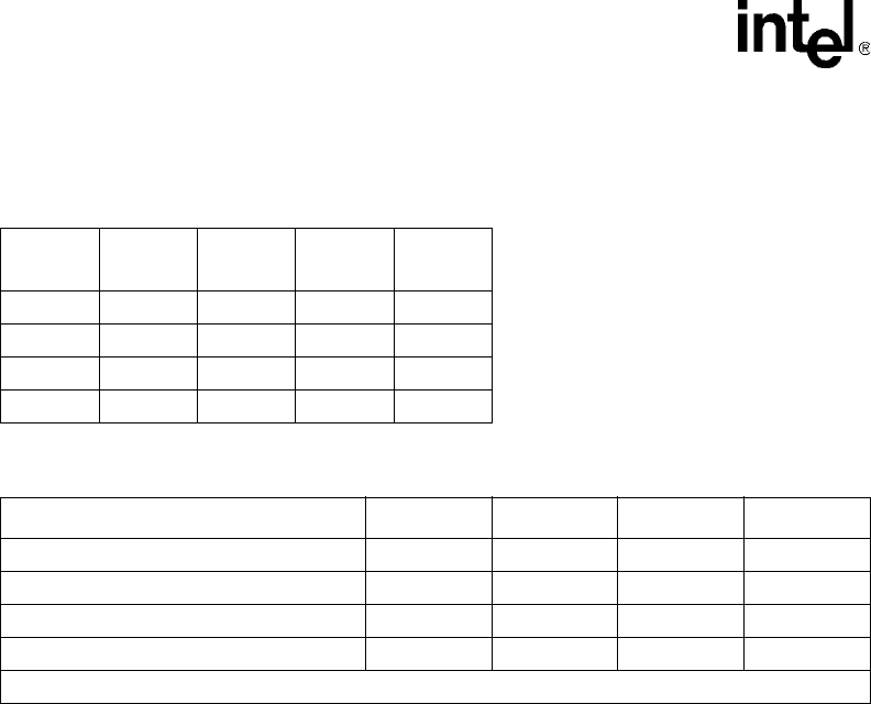
Table 60, shows the data in the registers for this example.
The value in Byte_Index[1:0] CSR (which controls the shift amount) for this example is 2.
As the examples show, byte aligning “n” words takes “n+1” cycles due to the first instruction
needed to start the operation.
Another mode of operation is to use the T_Index register with post-increment, to select the source
registers. T_Index operation is described later in this chapter.
4.3.2 CAM
The block diagram in Figure 59 is used to explain the CAM operation.
The CAM has 16 entries. Each entry stores a 32-bit value, which can be compared against a source
operand by instruction:
CAM_Lookup[dest_reg, source_reg].
All entries are compared in parallel, and the result of the lookup is a 9-bit value that is written into
the specified destination register in bits 11:3, with all other bits of the register set to 0 (the choice of
bits 11:3 is explained below). The result can also optionally be written into either of the LM_Addr
registers (see below in this section for details).
The 9-bit result consists of four State bits (dest_reg[11:8]), concatenated with a 1-bit Hit/Miss
indication (dest_reg[7]), concatenated with 4-bit entry number (dest_reg[6:3]). All other bits of
dest_reg are written with 0. Possible results of the lookup are:
• miss (0) — lookup value is not in CAM, entry number is Least Recently Used entry (which
can be used as a suggested entry to replace), and State bits are 0000.
• hit (1) — lookup value is in CAM, entry number is entry that has matched; State bits are the
value from the entry that has matched.
Table 60. Register Contents for Example 24
Register
Byte 3
[31:24]
Byte 2
[23:16]
Byte 1
[15:8]
Byte 0
[7:0]
03210
17654
2BA98
3FEDC
Example 25. Little-Endian Align
Instruction A Operand B Operand Prev A Result
Byte_align_le[--, r0] 3210 -- -- --
Byte_align_le[dest1, r1] 7654 3210 3210 5432
Byte_align_le[dest2, r2] BA98 7654 7654 9876
Byte_align_le[dest3, r3] FEDC BA98 BA98 DCBA
NOTE: B Operand comes from Prev_A register during byte_align_le instructions.