
Technical Advisory TA 1054


Copyright © 2014 Intel Corporation. * Other names and brands may be claimed as the property of others.
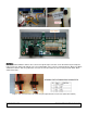
Figure 1. Location of the date code “P/N DD0S6CPB700 12/15/2013”
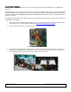
Figure 2. Location of the 2x12 pin connector (labeled “Main PWR1”) on the PDB
Root Cause
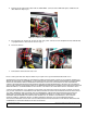
Intel has determined that this failure is due to the incorrectly wired pin connection on the two SATA 1x5 pin Peripheral
Power Connectors (labeled P5 and P6). The correct pin definition of the connector should be Orange, Black, Red, Black,
and Brown from Pin 1 while the problematic connectors are wired in a different order as Orange, Brown, Black, Black,
and Red from Pin 1.
Figure 3. Pin connection of the two SATA 1x5 pin Peripheral Power Connectors (labeled P5 and P6)