
Technical Product Specification


Chassis Power Sub-system Intel
®
Server Chassis P4000S Family TPS
Intel order number G22850-006 Revision 1.5
54
2.3.5.2 Over Voltage Protection (OVP)
The power supply over voltage protection shall be locally sensed. The power supply shall
shutdown and latces-off after an over voltage condition occurs. This latch shall be cleared by
toggling the PSON
#
signal or by an AC power interruption. The values are measured at the
output of the power supply’s connectors. The voltage shall never exceed the maximum levels
when measured at the power connectors of the power supply connector during any single point
of fail. The voltage shall never trip any lower than the minimum levels when measured at the
power connector. 12VSBwill be auto-recovered after removing OVP limit.
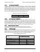
Table 64. Over Voltage Protection (OVP) Limits
Output Voltage
MIN (V)
MAX (V)
+12V
13.3
14.5
+12VSB
13.3
14.5
2.3.5.3 Over Temperature Protection (OTP)
The power supply will be protected against over temperature conditions caused by loss of fan
cooling or excessive ambient temperature. In an OTP condition the PSU will shut down. When
the power supply temperature drops to within specified limits, the power supply shall restore
power automatically, while the 12VSB remains always on. The OTP circuit must have built in
margin such that the power supply will not oscillate on and off due to temperature recovering
condition. The OTP trip level shall have a minimum of 4C of ambient temperature margin.
2.3.6 Control and Indicator Functions
The following sections define the input and output signals from the power supply.
Signals that can be defined as low true use the following convention: Signal
#
= low true
2.3.6.1 PSON# Input Signal
The PSON
#
signal is required to remotely turn on/off the power supply. PSON
#
is an active low
signal that turns on the +12V power rail. When this signal is not pulled low by the system, or left
open, the outputs (except the +5VSB) turn off. This signal is pulled to a standby voltage by a
pull-up resistor internal to the power supply. Refer Figure 31 for the timing diagram.
Table 65. PSON# Signal Characteristic
Signal Type
Accepts an open collector/drain input from the system.
Pull-up to VSB located in power supply.
PSON
#
= Low
ON
PSON
#
= High or Open
OFF
MIN
MAX
Logic level low (power supply ON)
0V
1.0V
Logic level high (power supply OFF)
2.0V
3.46V
Source current, Vpson = low
4mA
Power up delay: T
pson_on_delay
5msec
400msec
PWOK delay: T
pson_pwok
50msec