
Technical Product Specification


Chassis Power Sub-system Intel
®
Server Chassis P4000S Family TPS
Intel order number G22850-006 Revision 1.5
66
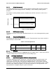
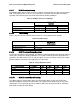
Table 86. Transient Load Requirements
Output
Max Step Load Size
Max Load Slew Rate
Test capacitive Load
+ 3.3VDC
5A
0.25 A/s
250 F
+ 5VDC
5A
0.25 A/s
400 F
+5Vsb
0.5A
0.25A/s
20 F
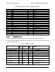
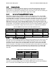
2.4.2.11 DC/DC Converter Capacitive Loading
The DC/DC converters are stable and meet all requirements with the following capacitive
loading ranges.
Min capacitive loading applies to static load only.
Table 87. Capacitive Loading Conditions
Converter output
Min
Max
Units
+3.3VDC
250
6800
F
+5VDC
400
4700
F
-12VDC
1
350
F
5Vstby
20
350
F
2.4.2.12 DC/DC Converters Closed Loop stability
Each DC/DC converter is unconditionally stable under all line/load/transient load conditions
including capacitive load ranges specified in section 2.4.2.11. A minimum of: 45 degrees phase
margin and -10dB-gain margin is required. The PDB provides proof of the unit’s closed-loop
stability with local sensing through the submission of Bode plots. Closed-loop stability must be
ensured at the maximum and minimum loads as applicable.
2.4.2.13 Common Mode Noise
The Common Mode noise on any output does not exceed 350mV pk-pk over the frequency
band of 10Hz to 20MHz.
The measurement shall be made across a 100Ω resistor between each of DC outputs,
including ground, at the DC power connector and chassis ground (power subsystem
enclosure).
The test set-up shall use a FET probe such as Tektronix* model P6046 or equivalent.
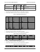
2.4.2.14 Ripple/Noise
The maximum allowed ripple/noise output of each DC/DC Converter is defined in the table
below. This is measured over a bandwidth of 0Hz to 20MHz at the PDB output connectors. A
10F tantalum capacitor in parallel with a 0.1F ceramic capacitor are placed at the point of
measurement.
Table 88. Ripple and Noise
+3.3V
+5V
-12V
+5VSB
50mVp-p
50mVp-p
120mVp-p
50mVp-p