
Technical Product Specification


Intel
®
Server Chassis P4000S Family TPS Chassis Power Sub-system
Revision 1.5 Intel order number G22850-006
65
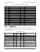
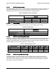
2.4.2.7 DC/DC Converters Loading
The following table defines power and current ratings of three DC/DC converters located on the
PDB, each powered from +12V rail. The 3 converters meet both static and dynamic voltage
regulation requirements for the minimum and maximum loading conditions.
Table 83. DC/DC Converters Load Ratings
+12VDC Input DC/DC
Converters
+3.3V Converter
+5V Converter
-12V Converter
MAX Load
15A
15A
0.5A
MIN Static/Dynamic Load
0A
0A
0A
Max Output Power
3.3V x15A =49.5W
5V x15A =75W
12V x0.5A =6W
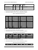
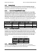
2.4.2.8 5VSB Loading
There is also one DC/DC converter that converts the 12V standby into 5V standby.
Table 84. 5VSB Loading
12V stby/5V stby
DC/DC Converters
MAX Load
5A
MIN Static/Dynamic Load
0.1
Max Output Power
5V x5A =25W
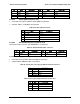
2.4.2.9 DC/DC Converters Voltage Regulation
The DC/DC converters’ output voltages stay within the following voltage limits when operating at
steady state and dynamic loading conditions. These limits include the peak-peak ripple/noise
specified in the table below. The 3.3V and 5V outputs are measured at the remote sense point,
all other voltages measured at the output harness connectors.
Table 85. Voltage Regulation Limits
Converter output
Tolerance
Min
Nom
Max
Units
+ 3.3VDC
-5%/+5%
+3.14
+3.30
+3.46
VDC
+ 5VDC
-5%/+5%
+4.75
+5.00
+5.25
VDC
- 12VDC
- 5%/+9%
-13.08
-12.00
-11.40
VDC
5Vstby
-5%/+5%
+4.75
+5.00
+5.25
VDC
2.4.2.10 DC/DC Converters Dynamic Loading
The output voltages remains within limits specified in table above for the step loading and
capacitive loading specified in the table below. The load transient repetition rate is only a test
specification. The step load may occur anywhere within the minimum load to the maximum
load shown in Table 83 and Table 84.