
Technical Product Specification


Intel
®
Server Chassis P4000S Family TPS Chassis Power Sub-system
Revision 1.5 Intel order number G22850-006
43
signal is pulled to a standby voltage by a pull-up resistor internal to the power supply.
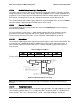
Refer to
Figure 27 for the timing diagram.
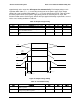
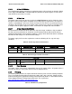
Table 47. PSON# Signal Characteristic
Signal Type
Accepts an open collector/drain input from the system. Pull-up
to VSB located in power supply.
PSON# = Low
ON
PSON# = High or Open
OFF
MIN
MAX
Logic level low (power supply ON)
0V
1.0V
Logic level high (power supply OFF)
2.0V
5.25V
Source current, Vpson = low
4mA
Power up delay: Tpson_on_delay
5msec
400msec
PWOK delay: T pson_pwok
50msec
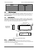
Figure 28. PSON# Required Signal Characteristic
2.2.7.2 PWOK (Power OK) Output Signal
PWOK is a power OK signal and will be pulled HIGH by the power supply to indicate that all the
outputs are within the regulation limits of the power supply. When any output voltage falls below
regulation limits or when AC power has been removed for a time sufficiently long so that power
supply operation is no longer guaranteed, PWOK will be de-asserted to a LOW state. Refer to
Figure 27 for a representation of the timing characteristics of PWOK.
The start of the PWOK
delay time shall be inhibited as long as any power supply output is in current limit.
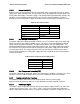
Table 48. PWOK Signal Characteristics
Signal Type
Open collector/drain output from power supply. Pull-up to VSB
located in system.
PWOK = High
Power OK
PWOK = Low
Power Not OK
MIN
MAX
Logic level low voltage, Isink=4mA
0V
0.4V
Logic level high voltage, Isource=200A
2.4V
5.25V
1.0 V PS
is enabled
2.0 V PS
is disabled
1.0V
2.0V
Enabled
Disabled
0.3V ≤ Hysteresis ≤ 1.0V
In 1.0-2.0V input voltages range is required
5.25V
0V