
Technical Product Specification


Intel
®
Server Chassis P4000S Family TPS Chassis Power Sub-system
Revision 1.5 Intel order number G22850-006
39
2.2.5.8 Residual Voltage Immunity in Standby mode
The power supply is immune to any residual voltage placed on its outputs (Typically a leakage
voltage through the system from standby output) up to 500mV. There is neither additional heat
generated, nor stressing of any internal components with this voltage applied to any individual
or all outputs simultaneously. It also does not trip the protection circuits during turn on.
The residual voltage at the power supply outputs for no load condition does not exceed 100mV
when AC voltage is applied and the PSON# signal is de-asserted.
2.2.5.9 Common Mode Noise
The Common Mode noise on any output does not exceed 350mV pk-pk over the frequency
band of 10Hz to 20MHz.
The measurement is made across a 100Ω resistor between each of DC outputs, including
ground at the DC power connector and chassis ground (power subsystem enclosure).
The test set-up shall use a FET probe such as Tektronix* model P6046 or equivalent.
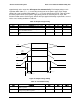
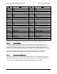
2.2.5.10 Ripple/Noise
The maximum allowed ripple/noise output of the power supply is defined in the table below. This
is measured over a bandwidth of 10Hz to 20MHz at the power supply output connectors. A
10F tantalum capacitor in parallel with a 0.1F ceramic capacitor is placed at the point of
measurement.
Table 43. Ripples and Noise
+3.3V
+5V
+12V 1, 2, 3
-12V
+5VSB
50mVp-p
50mVp-p
120mVp-p
200mVp-p
50mVp-p
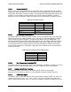
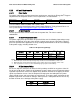
The test set-up shall be as shown below.
AC HOT
POWER SUPPLY
AC NEUTRAL
V
OUT
RETURN
V
AC GROUND
LOAD
SCOPE
LOAD MUST BE
ISOLATED FROM
THE GROUND OF
THE POWER
SUPPLY
10uF
.1uF
GENERAL NOTES:
1. LOAD THE OUTPUT WITH ITS MINIMUM
LOAD CURRENT.
2. CONNECT THE PROBES AS SHOWN.
3. REPEAT THE MEASUREMENTS WITH THE
MAXIMUM LOAD ON THE OUTPUT.
SCOPE NOTE:
USE A TEKTRONIX 7834 OSCILLOSCOPE WITH 7A13 AND
DIFFERENTIAL PROBE P6055 OR EQUIVALENT.
Figure 25. Differential Noise test setup
Note: When performing this test, the probe clips and capacitors should be located close to
the load.
2.2.5.11 Timing Requirements
These are the timing requirements for the power supply operation. The output voltages rise from
10% to within regulation limits (T
vout_rise
) within 2 to 50ms, except for 5VSB - it is allowed to rise
from 1 to 25ms. The +3.3V, +5V and +12V1, +12V2, +12V3 output voltages start to rise