Model 7200 Preliminary Service Manual Mainboard LED D/D & Charger Daughter Board LVDS : 77-72000-D02 77-72004-D00 77-7200C-D02 77-7200I-D10 77-720FL-D00 Specifications are subject to change without notice.
Specifications The Notebook Computer is a state-of-the-art, high performance, portable system. It offers a host of features specially designed to enhance performance and usability. l CPU ü ü ü l Memory ü ü ü ü ü Intel P54C Intel P54LM Intel P55C with MMX technology. 3.3 V power supply. Supports Fast Page Mode/EDO. 512KB secondary cache pipeline burst synchronous SRAM. 8MB expandable up to 128MB. 8/16/32/64MB 144-pin SODIMM RAM modules (option). l System BIOS ü 256KB flash ROM. ü PCI 2.1.
l PC Card Sockets ü One Type III or two Type II PC cards. ü CardBus support. ü One ZV-capable socket. l Mass Storage ü 2.5” (19mm high or less) or 3.0” (12.5mm high or less) hard disk drive. ü 3.5” floppy disk drive (interchangeable). ü 5.25” CD-ROM. ü 2.5” or 3.0” secondary hard disk drive. (option). l Infrared Wireless Communication ü IrDA. ü ASKIR. ü FIR. l Audio ü ü ü ü Sound Blaster Pro compatible. 3D stereo sound effects. Built-in microphone. 1MB ROM wavetable.
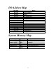
I/O Address Map Hex range 000 - 00F 020 - 021 040 - 043 048 - 04B 060 - 06E 070 - 071 080 - 08F 0A0 - 0A1 0C0 - 0DF 1F0 - 1F7 3F6 , 3F7 2F8 - 2FF 378 - 37A 3B4 , 3B5 3D4 , 3D5 3BA 3C0 - 3DA 3F2 - 3F7 3F0 , 3F1 3F8 - 3FF Device DMA controller-1 Interrupt controller-1 Timer 1 Timer 2 KB controller M38813 chip select RTC and NMI mask DMA page register Interrupt controller-2 DMA controller-2 Fixed disk select Serial port 2 Parallel port 1 CRT controller index (mono) CRT controller index (color) Feature control
Motherboard The motherboard is designed mainly based on Pentium CPU and the OPTi FireStar 82C700 chipset; it includes the following features: * OPTi 82C700 chipset solution from OPTi * C&T 65554 Multimedia Flat Panel Controller * PCI Local Bus IDE interface * SMC669FR super I/O Floppy Disk Controller * M38813 Keyboard Controller * Flash EPROM 256KB with AMI system BIOS, VGA BIOS * DRAM Upgradable to 128MB * 7 DMA channels * 13 interrupt levels * Real Time clock / calendar, battery back up * Buzzer for sound
Microprocessor P54C Pentium-100 Microprocessor The Intel Pentium Microprocessor is a 64-bit architecture with on chip Memory Management Unit (MMU), floating point (math coprocessor) and cache memory (16K bytes, code and data caches each contain 8 Kbytes of information) units. It has the same functions of the Pentium-75 CPU, but provides greatly enhanced performance.
Chips Core Logic Chip - OPTi FireStar 82C700 l l l l l l l l l l l l l l l l l l Support for Intel 586 CPU with bus speed up to 66MHz Support for both symmetric and asymmetric type DRAM High Performance Memory Controller Enhanced hidden refresh Support for Fast Page mode, EDO type.
VGA Controller - C&T 65554 l l l l l l l l l l l Supports displays with options for 1, 1.5, 2 and 4 MB Supports burst PCI and EDO/FPM. Supports 16 bit color DSTNs up to 1024x768x64K color, and TFT panels up to 1280x768x16M color. Supports non-interlaced 1280x1024x64K, 1024x768x16M, 800x600x16M, and 640x480x16M color on CRT Simultaneous display on flat panel and CRT.
PC CARD 95 (CardBus) Interface Controller - TI PCI1131 TI CardBus Interface Controller 1131 implements the PCMCIA 2.0/JEIDA 4.1 standard. It contains the following functions: l PCI interface Specification 2.
Super I/O Floppy Disk Controller - SMC FDC669FR l l l l l Intelligent Auto Power Management 16 Bit Address Qualification (Optional) 2.88MB Super I/O Floppy Disk Controller ü Support Vertical Recording Format ü 16 Byte Data FIFO ü Enhanced Digital Data Separator. Data rate up to 1Mb/s. Multi-Mode Parallel Port with ChiProtect Circuitry ü Standard Mode IBM PC/AT and PS/2 compatible bi-directional Parallel port.
AIT1108E VGA to NTSC/PAL Converter l l l Converts VGA source analog RGB into broadcast-quality NTSC or PAL video signal. Multiple output standards - NTSC, PAL. S-Video output format. Real PCI To USB (OHCI) Chip - CMD0670 l l l l l l l l l Complies with OpenHCI 1.0,USB 1.0,and PCI Local Bus 2.1 specifications. Bridges PCI bus and the Universal Serial Bus (USB). USB device bandwidth of up to 12 Mb/s. Full support of real time dynamic insertion and removal of devices. 32-bit PCI local bus interface.
ESS ES1879 High Quality Audio Chip l l l l Single,mixed-signal,16-bit stereo VLSI chip for digital audio High-quality,20-voice ESFM music synthesizer patents pending Supports ES978 Expansion audio Mixer chip Full Plug and Play (PnP) ES690 Wavetable Synthesizer l l l l Wavetable music synthesizer. Playback of 16-bit data at 44.1 KHz via the ES1xxx DAC. MIDI serial port compatible with MPU-401 serial port of ES1xxx. Glueless interface with the external wavetable ROM.
Interfaces Floppy Disk Drive Interface Pin 1 2 3 4 5 6 7 8 9 10 11 12 13 14 15 16 17 18 19 20 21 22 23 24 25 26 27 28 Description VCC VCC MTR0# INDEX# 3MOD FDD0# TRK0# DSKCHG# HDSEL# DIR# RDATA# STEP# WRPRT# WDATA# WGATE# DETECT0 GND GND N.C DETECT1 N.C N.C N.C N.C N.C N.C N.C N.C Pin 29 30 31 32 33 34 35 36 37 38 39 40 41 42 43 44 45 46 47 48 49 50 51 52 53 54 55 56 13 Description N.C N.C N.C N.C N.C N.C N.C N.C GND GND N.C N.C N.C N.C N.C N.C N.C N.C N.C N.C N.C N.C N.C N.C N.C N.
Hard Disk Drive Interface The Notebook PC has a standard PC/AT interface (IDE) which can directly interface with any hard disk drive with an embedded controller supporting the same PC/AT interface through the use of a 56-pin B/B connector. The 56-pin connector has the following pin configurations: Pin 1 2 3 4 5 6 7 8 9 10 11 12 13 14 15 16 17 18 19 20 21 22 23 24 25 26 27 28 Description VCC VCC N.C N.C N.C N.C N.C N.C N.C N.C N.C N.C N.C N.C N.
RS-232C Serial Interface The Notebook PC has one RS-232C serial port which enables users to connect a serial printer, a serial mouse, a plotter, a modem, etc.
Expansion Memory Socket The Notebook PC has two 144-pin SODIMM type Expansion memory sockets with the following pin configurations: Socket 1: Pin 1 4 7 10 13 16 19 22 25 28 31 34 37 40 43 46 49 52 55 58 61 64 67 70 73 76 79 82 85 88 91 94 97 100 103 106 109 112 115 118 121 124 127 130 133 136 139 142 Description GND MD32 MD2 MD35 MD4 MD37 MD7 GND ICAS#1 MEM-VCC IMA1 IMA5 MD8 MD41 MD11 MEM-VCC MD13 MD46 GND N.C MEMCLK1 MEM-VCC IMWE# MEMCLK2 GND GND N.
Socket 2: Pin 1 4 7 10 13 16 19 22 25 28 31 34 37 40 43 46 49 52 55 58 61 64 67 70 73 76 79 82 85 88 91 94 97 100 103 106 109 112 115 118 121 124 127 130 133 136 139 142 Description GND MD32 MD2 MD35 MD4 MD37 MD7 GND ICAS#1 MEM-VCC IMA1 IMA5 MD8 MD41 MD11 MEM-VCC MD13 MD46 GND N.C MEMCLK3 MEM-VCC IMWE# MEMCLK4 GND GND N.C MEM-VCC MD17 MD50 GND MD52 MD22 MD55 IMA6 IMA11 IMA9 N.
Docking Connector Pin Assignment Pin 1 4 7 10 13 16 19 22 25 28 31 34 37 40 43 46 49 52 55 58 61 64 67 70 73 76 79 82 85 88 91 94 97 100 103 106 109 112 115 118 121 124 127 130 133 136 139 142 145 148 151 154 157 160 163 166 Description A+ SOUTA /DSR2 GND PPD0 /INIT SLCT GND CCLK1 GND CCO GND /DTR2 /SLCTIN PPD5 /ACK BHSYNC RED DDCDATA DSRA DCDA CAD30 CC/BE#0 CGNT1# CAD15 CAD6 MTR0# FDD1# FB0 RIA CINTB# CAD16 CGNT2# CREQ3# CAD8 TRK0# WRPRT# DOCKEN# CINTC# CAD25 CAD21 CSERR# CBLOCK# CAD10 CAD1 DIR# 3MOD-B SE
Internal Trackpad Interface There is a 8-pin connector used to interface with the internal trackpad. It will be disabled when external mouse has been installed. The trackpad is hardwareconnected to PS/2 port, hardware-compatible to Microsoft PS/2 mouse and softwarecompatible to Microsoft mouse mode. The following is the pin configuration for the connector: Pin 1 2 3 4 5 6 7 8 Description VCC PS/2 DATA PS/2 CLK SW Right SW Left GND N.C N.
External Keyboard/PS2 Mouse Interface Pin 1 2 3 4 5 6 Description KBD-DATA MUS-DATA GND VCC KBD-CLK MUS-CLK External S-Video TV-Out Interface Pin 1 2 3 4 Description GND GND XLUMA XCRMA External Game Port Interface Pin 1 2 3 4 5 6 7 8 9 10 11 12 13 14 15 Description VCC SWA TA GND GND TB SWB VCC VCC SWC TC MSO TD SWD MSI 20
External USB (Universal Serial Bus) Interface Port A: Pin 1 2 3 4 Description V1+OUT VD1-N VD1-P GND Pin 1 2 3 4 Description V2+OUT VD2-N VD2-P GND Port B: 21
Internal ISA Interface (For Optional Modem/LAN) Pin 1 2 3 4 5 6 7 8 9 10 11 12 13 14 15 16 17 18 19 20 21 22 23 24 25 26 27 28 29 30 Description RSTDRV SD0 SD2 SD4 SD6 SD8 SD10 SD12 VCC SD14 SMEMR# IO16# IORD# IOWR# IRQ3 IRQ4 IRQ5 IRQ9 SA0 SA2 SA4 SA6 SA8 SA10 SA12 SA14 SA16 SA18 GND MIC-IN Pin 31 32 33 34 35 36 37 38 39 40 41 42 43 44 45 46 47 48 49 50 51 52 53 54 55 56 57 58 59 60 22 Description MODEM SD1 SD3 SD5 SD7 SD9 SD11 SD13 VCC SD15 IOCHRDY +12V AEN IRQ10 IRQ11 IRQ12 3.3V 3.
Internal Hardware MPEG Interface (For Optional MX501/ALi3307) Pin 1 2 3 4 5 6 7 8 9 10 11 12 13 14 15 16 17 18 19 20 21 22 23 24 25 26 27 28 29 30 Description VCC GND AD0 AD2 AD4 AD6 AD8 AD10 AD12 AD14 AD16 AD18 AD20 AD22 AD24 AD26 AD28 AD30 GND CBE#0 CBE#2 PCIRST# GND PCICLK5 GND FRAME# IRDY# TRDY# AD19 VCC Pin 31 32 33 34 35 36 37 38 39 40 41 42 43 44 45 46 47 48 49 50 51 52 53 54 55 56 57 58 59 60 23 Description VCC GND AD1 AD3 AD5 AD7 AD9 AD11 AD13 AD15 AD17 AD19 AD21 AD23 AD25 AD27 AD29 AD31 GND CB
PCMCIA CardBus Interface Socket A: Pin 1 2 3 4 5 6 7 8 9 10 11 12 13 14 15 16 17 18 19 20 21 22 23 24 25 26 27 28 29 30 31 32 33 34 Description GND A-CD3 A-CD4 A-CD5 A-CD6 A-CD7 A-CE1# A-CA10 A-OE# A-CA11 A-CA9 A-CA8 A-CA13 A-CA14 A-WE# A-RDYBY# A-VCC-C A-VPP A-CA16 A-CA15 A-CA12 A-CA7 A-CA6 A-CA5 A-CA4 A-CA3 A-CA2 A-CA1 A-CA0 A-CD0 A-CD1 A-CD2 A-WP# GND Pin 35 36 37 38 39 40 41 42 43 44 45 46 47 48 49 50 51 52 53 54 55 56 57 58 59 60 61 62 63 64 65 66 67 68 24 Description GND A-CD1# A-CD11 A-CD12 A-CD1
Socket B: Pin 1 2 3 4 5 6 7 8 9 10 11 12 13 14 15 16 17 18 19 20 21 22 23 24 25 26 27 28 29 30 31 32 33 34 Description GND B-CD3 B-CD4 B-CD5 B-CD6 B-CD7 B-CE1# B-CA10 B-OE# B-CA11 B-CA9 B-CA8 B-CA13 B-CA14 B-WE# B-RDYBY# B-VCC-C B-VPP B-CA16 B-CA15 B-CA12 B-CA7 B-CA6 B-CA5 B-CA4 B-CA3 B-CA2 B-CA1 B-CA0 B-CD0 B-CD1 B-CD2 B-WP# GND Pin 35 36 37 38 39 40 41 42 43 44 45 46 47 48 49 50 51 52 53 54 55 56 57 58 59 60 61 62 63 64 65 66 67 68 25 Description GND B-CD1# B-CD11 B-CD12 B-CD13 B-CD14 B-CD15 B-CE2# B-
LCD Interface (For TFT XGA With FPDL/Panel Link) Connector A: Pin 1 2 3 4 5 6 7 8 9 10 11 12 13 14 15 16 17 18 19 20 21 22 23 24 25 26 27 28 29 30 Description GND GND PP0 PP2 PP4 PP6 PP8 PP10 PP12 PP14 PP16 PP18 PP20 GND GND PP22 VCC VCC PP24 PP26 3.3V 3.3V M LCDVCC CONTADJ LCDVDD LCDVDD SHFCLK GND GND Pin 31 32 33 34 35 36 37 38 39 40 41 42 43 44 45 46 47 48 49 50 51 52 53 54 55 56 57 58 59 60 26 Description GND GND PP1 PP3 PP5 PP7 PP9 PP11 PP13 PP15 PP17 PP19 PP21 GND GND PP23 VCC VCC PP25 PP27 3.
Connector B: Pin 1 2 3 4 5 6 7 8 9 10 11 12 13 14 15 16 17 18 19 20 21 22 23 24 25 26 27 28 29 30 Description GND GND DEDGE TxVCC TxVCC TEST TxAVCC TxAVCC VMA3 100DVCC VMA5 TxPVCC EXT-RES GND GND SUPV A- VCC A- VCC PP28 PP30 PP32 PP34 A-- VCC A-- VCC ENABKL N.C B+ B+ N.
DC/DC Converter Board The Notebook PC has a built-in DC/DC converter module which provides all the DC voltage outputs required by the system. This module will have the following features: A. Input requirements : - Voltage input from AC adapter : - Voltage input from battery : B. Output Requirements : Voltage Regulation +5V -4% ~ +2% +3.3V -4% ~ +2% +12V -5% ~ +5% 20.0V 12.0V (Ni-MH), or 10.8V (Li-Ion) Ripple & Noise 100mV P-P 100mV P-P 200mV P-P Current Peak 3.0A 5.0A 400mA Current Min. 0.5A 0.5A 0.
CPU Power Board The module provides special CPU which voltage is adjustable (from 1.5V - 3.1V), This module will have the following features : A. Input requirement : - Voltage input from AC adapter :+20V. - Voltage input from battery :+12V (Ni-MH), or +10.8V (Li-Ion) B. Output requirement : Voltage 1.5V - 3.1V Regulation -4%- +2% Ripple & noise 100mV P-P Current 4A Current:typical 3A C. Efficiency : The total efficiency is 85% minimum at typical load condition. D.
Inverter Board The Notebook PC has a built-in inverter module which provides all the requirements to support the DSTN color and TFT color panels. This module will have the following features: DC input: 8V ~ 21V full range AC output: Item Input voltage (V) Input current (A) Non-load output voltage (V) Frequency (KHz) Output current (mA) Output voltage Min. 8 Typical 1000 40 2 1200 50 5 30 Max. 21 0.
Setting DIP Switch Locate the DIP Switch (SW1) to set the correct configuration for the following purposes: l Flash ROM BIOS Update. l CPU upgrade. l Cache mode (reserved).
POST Checkpoint Codes POST is performed by the BIOS when the computer is reset or booted. POST tests and initializes key components. When a POST routine completes, a code is written to I/O port address 80h. Display this code by attaching diagnostic equipment to I/O port address 0080h. Uncompressed Initialization Codes Code D0h D1h D3h D4h D5h D6h D7h D8h D9h Description The NMI is disabled. Power on delay is starting. Next, the initialization code checksum will be verified.
Power On Self Test POST Phases Every time the system is power on, BIOS executes two types of POST routines: System Test and Initialization System Configuration Verification Test and initialize BIOS for normal operations. Compare defined configuration with hardware actually installed. BIOS Error Reporting If an error occurs before the display device is initialized, a series of audio beeps will be emitted to indicate that a fatal error is detected.
If an error occurs after the display device is initialized, the error message is displayed. A prompt to press will appear with the displayed error message. Error Message 8042 Gate - A20 Error Address Line Short C: Drive Error C: Drive Failure Cache Memory Bad, Do Not Enable Cache.
Invalid Boot Diskette Keyboard Is Locked…Unlock It Keyboard Error KB/Interface Error No ROM BASIC Off Board Parity Error On Board parity Error Parity Error ??? The BIOS can read the disk in the floppy disk drive A:, but can not boot the computer. Use another boot disk. The keyboard lock is engaged. The computer must be unlocked to continue. There is a timing problem with the keyboard. Set the keyboard option in Standard Setup to Not Installed to skip the keyboard POST routines.