
ITP700 Debug Port Design Guide

R
26 ITP700 Debug Port Design Guide
There are three signal groups within the debug port. Each group has a different set of layout
requirements:
• System - The system signal group indicates the access state of the entire system
• JTAG - The JTAG signal group consists of the five standard JTAG pins. The JTAG signals
are to be designed to run up to 16 MHz.
• Execution - The execution signal group contains the reset and run control signals used to
indicate operational conditions.
The following three subsections clarify the routing guidelines for each of these signal classes.
VTERM is the termination voltage of the system bus BPM[5:0]# and RESET# signals defined in
the processor datasheet. VTAP refers to the pull-up voltage of the JTAG signals on the system
board. This pull-up voltage is chosen by the system designers to be consistent with the JTAG IO
buffer specs for the processor and the ITP. Information on input voltage specifications, drive
strength, and recommended termination values for the processor can be obtained from processor
datasheets. VTAP should be used for the pull-up resistors on all JTAG signals in the scan chain
that operates directly from the ITP. If a bus translator is used to translate an ITP scan chain to a
higher voltage, VTAP on the opposite side of the translator from the ITP shall change as well.
Note: Note that all termination locations indicated are referenced to the target system.
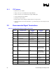
2.3.1 System Signal Layout Guidelines
Table 11. System Signal Layout Guidelines
Debug Port Signal Layout Guideline
PWR If PWR is used to arbitrate with a local TAP master for control of the scan
chain: Pull-up resistor to VTERM and an open drain control gate must be
located less than 1 ns from the debug port.
If PWR is not used to arbitrate with a local TAP master for control of the
scan chain: Pull-up resistor to VTERM must be located less than 1 ns from the
debug port.
BCLK(p/n)
1.
BCLK for the debug port should originate as a unique output of the system
clock tree. The BCLK routed from the clock distribution component to the debug
port must have a propagation delay equal to the length of the BCLK traces from
the clock distribution component to the other front side bus agents plus the
electrical length of the BPM[5:0]# and RESET# signals as measured from the
nearest system bus agent to the debug port. This will ensure that these critical
signals have the same phase relationship at the debug port as is seen at the
processor.
BCLK is a differential high speed clock supplied by the target system. It is a
critical system signal requiring careful timing and signal integrity considerations.
FBO FBO is used to monitor the phase relationship of TCK to BCLK and to recover
TDO. It is important that the phase of FBO to BCLK at the debug port is the
same as the phase of TCK to BCLK at the closest system bus agent. To meet
this requirement, the electrical length fixed by BPM[5:0]# and RESET#
(between the nearest bus agent routed to the debug port) must also be the
electrical length of FBO(TCK) from the closest bus agent back to the debug
port. See the Execution Signal Layout Guidelines in this chapter for additional
information.