
Embedded Voltage Regulator-Down (EmVRD) 11.0 Design Guidelines for Embedded Implementations Supporting PGA478

EmVRD 11.0—10.0
Embedded Voltage Regulator-Down (EmVRD) 11.0
Design Guidelines for Embedded Implementations January 2007
46
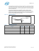
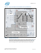
10.3.2 Ganging Common Pins
To maximize the benefit of using the top layer for V
CC
delivery, the power shape should
directly capture all possible socket V
CC
pads. Using the pattern shown in Figure 17
allows the V
CC
shape to flow through both sides of the CPU socket and make direct
connection with the mid-frequency decoupling capacitors in the socket cavity. Also
shown is the ganging of the V
SS
pads to lower the inductance to the GND layers.
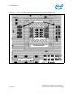
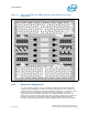
Figure 16. Layer 10 V
CC
Shape For Intel’s Reference Ten Layer Motherboard
PGA 478 Socket
V
CCP
Shape
MLCC Bypass
V
CC
Core Shape