
Embedded Voltage Regulator-Down (EmVRD) 11.0 Design Guidelines for Embedded Implementations Supporting PGA478

EmVRD 11.0—10.0
Embedded Voltage Regulator-Down (EmVRD) 11.0
Design Guidelines for Embedded Implementations January 2007
44
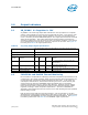
path to the processors. Using the bottom and internal layers where possible to provide
CPU core planes is also recommended. A complete stack-up example of processor
reference board is provided in Table 20.
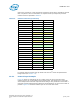
Note: Table does not show the scale of layer thickness.
For further reference board stack-up details see the Intel
®
E7520 Chipset Platform
Design Guide (see Section 1.3).
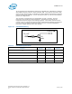
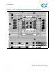
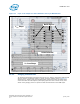
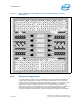
10.3.1 Power Shape Example
Figure 15 shows an example of the V
CC
shape on the top layer of the processor
reference board. To accommodate testing attachments, this design has a larger CPU
socket keepout than would be required normal designs. The placement of the VR11.0
inductors and the bulk decoupling capacitors should ideally be as close to the socket as
possible. Figure 16 shows the bottom layer for the same CPU socket.
Table 20. Reference Board Layer Stack-up
Layers Material Thickness (mils)
Soldermask 1.0
Plating 1.4
L1 (Top-PWR) Copper 0.6
Prepreg 4.0
L2 (Plane-GND) Copper 1.2
Core 4.0
L3 (Signal) Copper 0.6
Prepreg 6.0
L4 (Plane-GND) Copper 1.2
Core 4.0
L5 (Signal) Copper 0.6
Prepreg 25.0
L6 (Signal) Copper 0.6
Core 4.0
L7 (Plane-GND) Copper 1.2
Prepreg 6.0
L8 (Signal) Copper 0.6
Core 4.0
L9 (Plane-GND) Copper 1.2
Prepreg 4.0
L10 (Bottom-PWR) Copper 0.6
Plating 1.4
Soldermask 1.0