
Embedded Voltage Regulator-Down (EmVRD) 11.0 Design Guidelines for Embedded Implementations Supporting PGA478

Embedded Voltage Regulator-Down (EmVRD) 11.0
January 2007 Design Guidelines for Embedded Implementations
43
10.0—EmVRD 11.0
10.0 Mother Board Power Plane Layout
The motherboard layer stack-up must be designed to ensure robust, noise-free power
delivery to the processor. Failure to minimize and balance power plane resistance may
result in non-compliance to the processor load line specification. A poorly planned
stack-up or excessive holes in the power planes may increase system inductance and
generate oscillation on the Vcc voltage rail at the processor. Both of these types of
design errors can lead to processor failure and must be avoided by careful V
CC
and V
SS
plane layout and stack-up. The types of noise introduced by these errors may not be
immediately observed on the processor power pins or during system-board voltage
transient validation, so issues must be resolved by design, prior to layout, to avoid
unexpected failures.
Following basic layout rules can help avoid excessive power plane noise. All
motherboard layers in the area surrounding the processor socket should be used for
V
CC
power delivery; copper shapes that encompass the power delivery region of the
processor pin field are required. A careful motherboard design will help ensure a well-
functioning system that minimizes the noise profile at the processor die. The following
subsections provide further guidance.
10.1 Minimize Power Path DC Resistance
Power path resistance can be minimized by ensuring that the copper layout area is
balanced between V
CC
and V
SS
planes. A good board design will have two V
CC
layers
and a minimum of two Vss layers. Because there is generally more V
SS
copper in the
motherboard stack-up, care should be taken to maximize the copper in V
CC
floods.
This includes care to minimize unnecessary plane splits and holes when locating
through hole components, vias, and connection pads.
10.2 Minimize Power Delivery Inductance
At higher frequencies the ordering of the motherboard layers becomes critical as it is
V
CC
/V
SS
plane pairs which carry current and determine power plane inductance. The
layer stack-up should maximize adjacent (layer-to-layer) planes at a minimized spacing
to achieve the smallest possible inductance. Care must be taken to minimize
unnecessary plane splits and holes when locating through-hole components, vias, and
connection pads. Minimized inductance will ensure that the board does not develop low
frequency noise which may cause the processor to fail (load line violation).
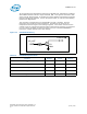
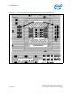
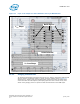
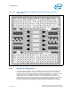
10.3 Ten Layer Board
In embedded applications, the nominal layer count for a control board is normally much
higher than the standard desktop or commodity server boards. An example will be
shown for a ten layer board that provides four routing layers, four ground layers, and
two outer layers for power. The use of the top and bottom layers for power is becoming
increasingly important as the transition speed of current demand has increased.
Providing generous voltage planes on the top layer directly from the VR11.0 output
inductors to the CPU socket provides the lowest possible resistance and inductance