
Embedded Voltage Regulator-Down (EmVRD) 11.0 Design Guidelines for Embedded Implementations Supporting PGA478

Embedded Voltage Regulator-Down (EmVRD) 11.0
January 2007 Design Guidelines for Embedded Implementations
41
9.0—EmVRD 11.0
9.0 Output Indicators
9.1 VR_READY: V
CC
Regulator Is ‘ON’
VR_READY is an active high output that indicates the start-up sequence is complete
and the output voltage has moved to the programmed VID value. This signal is used
for start-up sequencing for other voltage regulators, the clock, and microprocessor
reset. It is tied to processor PWRGOOD input pin. This signal should not be de-asserted
during D-VID operation. The signal should remain asserted during normal DC-DC
operating conditions and only de-assert for fault or shutdown conditions. This signal is
not a representation of the accuracy of the DC output to its VID value. See Figure 10
for timing and Table 18 for signal specifications.
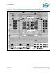
9.2 FORCEPR# and EmVRD Thermal Monitoring
Each customer is responsible for identifying maximum temperature specifications for all
components in the voltage regulator design and ensuring that these specifications are
not violated while continuously drawing specified VR_TDC levels. In the event of a
catastrophic thermal failure, the thermal monitoring circuit is to assert the VR_HOT
signal to drive the processor FORCEPR# input immediately prior to exceeding
maximum temperature ratings to prevent heat damage. Assertion of these signals
lowers processor power consumption and reduce current draw through the voltage
regulator, resulting in lower component temperatures. Assertion of FORCEPR#
degrades system performance and must never occur when drawing less than specified
thermal design current.
Both VR_HOT and VR_FAN are active high outputs. See the controller IC vendor’s
datasheets for signal interface specifications (open drain or push-pull). VR_HOT cannot
be tied directly to FORCEPR#; the signal must be inverted and buffered. See Figure 14
for buffering information and Table 19 for FORCEPR# signal requirements.
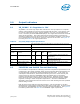
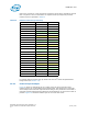
Table 18. VR_Ready Output Signal Specifications
Signal Type
Open Collector/Drain Logic output from PWM IC, with external pull-up resistor and
reference voltage.
VR_Ready = HIGH Active / Asserted
VR_Ready = LOW Not Active / De-Asserted
Symbol Parameter Min Max Units Remarks
VOH Output Voltage High 0.8 1.6 V
V
CCP
rail is expected; Open Coll./Drain Trans.
OFF, Imp. >100k depending on system
implementation
VOL Output Voltage Low 0 0.3 V
With external pull-up resistor;
Open Coll./Drain Trans. ON
IOL Output Low Sink Current 1.0 4.0 mA DC Current limit set by external pull-up resistor
Transition Edge Rate 150 ns From 10-90% rise