
Embedded Voltage Regulator-Down (EmVRD) 11.0 Design Guidelines for Embedded Implementations Supporting PGA478

Embedded Voltage Regulator-Down (EmVRD) 11.0
January 2007 Design Guidelines for Embedded Implementations
35
6.0—EmVRD 11.0
6.0 Control Inputs
6.1 Voltage Identification (CPU VID [5:0], EmVRD [6:1])
The EmVRD controller must accept an 8-bit code transmitted by the processor to
establish the reference V
CC
operating voltage. VR 11.0 based controllers support both
VR10.x and VR11.0 VID tables, only the VR11.0 will be used by the processors and will
be discussed in this document.
The processors use six VID pins. To match the VID resolution least significant bit in the
processor to EmVRD controller, the VID signals are shifted up by one from CPU to
EmVRD controller. The two unused VID inputs should be grounded. The VID
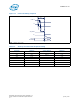
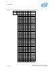
connections are shown at the top of Table 17.
When an ‘OFF’ VID code appears at the input to the EmVRD controller, the DC-DC
should turn off the V
CC
output within 0.5 seconds and latch off until power is cycled.
Since the processor VID map uses all zeros as the only off condition, the VID bits
should use pull down resistors. This will keep the VR off with an empty processor
socket.
While operating in the D-VID mode, the processor can transmit VID codes across the
six bit bus with a 5 ms data transmission rate. To properly design this bus against
timing and signal integrity requirements, the following information is provided. The
VID buffer circuit in the processor use a push-pull CMOS circuit configuration. The
worst-case settling time requirement for code transmission at each load is 400 ns,
including line-to-line skew. EmVRD controller VID inputs will contain circuitry to detect
a change and prevent false tripping or latching of VID codes during this 400-
nanosecond window.
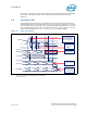
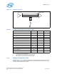
Intel recommends use of the D-VID bus topology described in Figure 13 and Table 16.
Under these conditions, traces can be routed with microstrip, stripline, or a
combination with a maximum of four layer transitions. The main trace length can vary
between ½ inch and 15 inches with a maximum recommended line to line skew of 1
inch. The 2 k
Ω +/-10% pull-down resistor can be placed at any location on the trace
with a maximum stub length of 1 inch.
Some designs may require additional VID bus loads. In this case, care should be taken
to design the topology to avoid excessive undershoot and overshoot at each load.
Failure to comply with these limits may lead to component damage or cause premature
failure. The responsible engineer must identify minimum and maximum limits of each
component and design a topology that ensures voltages stay within these limits at all
times.