
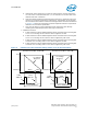
Embedded Voltage Regulator-Down (EmVRD) 11.0 Design Guidelines for Embedded Implementations Supporting PGA478

EmVRD 11.0—4.0
Embedded Voltage Regulator-Down (EmVRD) 11.0
Design Guidelines for Embedded Implementations January 2007
30
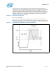
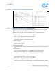
4.0 Power Sequencing
EmVRD 11.0 features a power sequence that is compatible with both VR11 and VR10
processors. To avoid compatibility problems with VR11 architecture, EmVRD 11.0
systems must not use the legacy VR10 start sequence.
Embedded VR11 systems can use a pull-up resistor tied to the V
CCP
supply as an enable
signal or provide additional sequencing or check circuits before enabling. Once the PWM
V
CC
voltage is above its UVLO threshold and out of reset or configuration states and a
valid enable signal is received, the PWM can initiate the start up sequence with TD1.
The EmVRD should ramp V
CC
to the default ‘Vboot’ value and start its internal timer. It
will remain at the Vboot voltage during TD3 and then read in the VID lines and ramp to
the VID programming voltage. Vboot is a DC voltage state with no load line or AVP
function. See timing diagram Figure 12 for details on the power-on sequence
requirements.
4.1 VR_ENABLE
VR_ENABLE pin is a level sensitive logic input that is externally pulled up to the front
side bus termination voltage rail (V
CCP
) rail in the system. The threshold for turn on is
0.85 V +/- 50 mV with a 100 mV +/- 30 mV hysteresis. The VR_ENABLE input should
have a 3 dB bandwidth of approximately 20 MHz to reject high frequency noise. If
enable goes low during the start up sequence the EmVRD should re-start the start up
sequence.
When VR_ENABLE is pulled low or disabled, VR_READY should be de-asserted and the
DC-DC output should be in a high-impedance state and should not sink current. During
the shut down process, no negative voltage below –100 mV may be present at the DC-
DC output when loaded with a resistive load or microprocessor in the system. Some
electronic loads with long leads may cause false readings at turn off.
4.2 Vboot Voltage Level
Vboot is a default power-on V
CC
value. Upon detection of a valid Vccp supply, the
EmVRD controller is to regulate the output to this value until VID codes are read. The
Vboot voltage is 1.1 V. During Vboot, the output should operate with no load line and as
if the VID code represents 1.1 V.
4.3 Under Voltage Lock Out (UVLO)
The EmVRD controller should detect the V
CC
input and remain in the disabled state until
valid V
CC
level is available or reached. Typically 3.0 V in a 3.3 V system, 4.0 V in a 5 V
system or 7 V to 8 V in a 12 V system. Ultimately the controller vendor should set the
level to meet applicable market segment requirements. However, the controller and
driver chips (in not integrated in the controller) should coordinate start up such that
both the EmVRD V
CC
and power conversion rail (typically +12 V) of the buck converter
are both up and valid prior to enabling the controller function. The controller and driver
combination need to be tolerant of any sequencing combination of 3.3 V, 5 V or 12 V