
Embedded Voltage Regulator-Down (EmVRD) 11.0 Design Guidelines for Embedded Implementations Supporting PGA478

EmVRD 11.0—2.0
Embedded Voltage Regulator-Down (EmVRD) 11.0
Design Guidelines for Embedded Implementations January 2007
26
2.7 EmVRD Output Filter
Embedded processor voltage regulators include an output filter consisting of large bulk
decoupling capacitors to compensate for large transient voltage swings and small value
ceramic capacitors to provide high frequency decoupling. This filter must be designed
to stay within load line specifications (Figure 1 and Table 3) across tolerances due to
age degradation, manufacturing variation, and temperature drift.
2.7.1 Bulk Decoupling
Bulk decoupling is necessary to maintain V
CC
within load line limits prior to the EmVRD
controller response. Design analysis shows that bulk decoupling greatly depends on
number of EmVRD phases and the FET switching frequency. Design analysis
determined that the most cost efficient filter solution incorporates bulk capacitors with
low (9 m
Ω) average ESR.
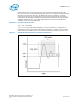
The D-VID mode of operation is directly impacted by the choice of bulk capacitors and
output inductor value in the EmVRD output filter. It is necessary to minimize V
CC
settling time during D-VID operation to hasten the speed of core temperature
reduction. The speed of recovery is directly related to the RCL time constant of the
output filter. To ensure an adequate thermal recovery time, it is recommended to
design the output filter with a minimal output inductor value and a minimal amount of
bulk capacitance with minimum ESR, while providing a sufficient amount of decoupling
to maintain load line and ripple requirements. At this time, high-density aluminum poly
capacitors with 9 m
Ω average ESR have been identified as the preferred solution.
Failure to satisfy the Vcc settling time requirements defined in Section 2.5 may
invalidate processor thermal modes; this may require a processor cooling solution (fan/
heatsink) that is more robust than recommended.
Through pre-silicon simulations of the embedded processor, the bulk decoupling
capacitor value of 330 µF shows the best performance. For each processor socket use
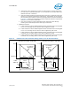
six bulk capacitors spaced evenly with three on both sides of the CPU socket where the
power pins reside. Place the bulk capacitors as close to the socket as possible and on
the top layer.
For the latest recommendations always consult the appropriate platform design
guideline for an output filter design capable of satisfying load line and D-VID
constraints.
2.7.2 High Frequency Decoupling
The output filter includes high frequency decoupling to ensure ripple and package noise
is suppressed to specified levels. Ripple limits are defined in section Section 2.3 and
package noise limits are defined in appropriate processor datasheets in the form of a
processor load line.
High frequency noise and ripple suppression are best minimized by 22 µF multi-layer
ceramic capacitors (MLCCs). It is recommended to maximize the MLCC count in the
socket cavity on the top layer to help suppress transients. Remaining MLCCs should be
placed adjacent to the socket edge and on the bottom of the board in the socket cavity
region and around the edge of the socket vias.
Intel recommends a high frequency filter consisting of MLCCs distributed uniformly
through the socket cavity region with a total equivalent ESR of 0.1 m
Ω and total
capacitance of 660 µF. The cavity-capacitor ESL value is not a sensitive parameter, but
Intel recommends minimizing the value to suppress noise. To ensure functionality with
all Intel processors, adoption of the reference solution (defined in appropriate Platform
Design Guides) accompanied by full processor load line validation is strongly
recommended. Contact your Intel sales representative to gain access to Platform
Design Guide documentation.