
Embedded Voltage Regulator-Down (EmVRD) 11.0 Design Guidelines for Embedded Implementations Supporting PGA478

EmVRD 11.0—2.0
Embedded Voltage Regulator-Down (EmVRD) 11.0
Design Guidelines for Embedded Implementations January 2007
18
2.3.5 Error Amp Specification
The EmVRD controller chosen should provide an error amp with a sufficient gain BW
product to ensure duty cycle saturation does not occur with large signal current
transients. Typical target closed loop VR bandwidths of 30-200 kHz (20% of switching
frequency target) are expected in EmVRD 11.0 system designs. The output of the error
amp should also have high slew rates to avoid duty cycle saturation. Performance
limitations must be included in the EmVRD TOB equations.
2.4 Stability
The EmVRD chosen should be unconditionally stable under all DC and transient
conditions across the voltage and current ranges defined in Table 4 and Figure 1. The
EmVRD must also operate in a no-load condition: i.e., with no processor installed.
Normally the no-processor VID code will be 00000, disabling the EmVRD output
voltage.
2.5 Dynamic Voltage Identification
2.5.1 Dynamic-Voltage Identification Functionality
EmVRD 11.0 architecture includes the Dynamic Voltage Identification (D-VID) feature
set, which enables the processor to reduce power consumption and processor
temperature. Reference VID codes are dynamically updated by the processor to the
EmVRD controller via the VID bus when a low power state is initiated. VID codes are
updated sequentially in 12.5 mV steps and are transmitted every 5 microseconds until
the final voltage code is encountered. Intel processors are capable of transitioning from
standard operational VID levels to the EmVRD 11.0 table minimum values. They are
also capable of returning to a higher VID code in a similar manner. The low voltage
code will be held for a minimum of 50 microseconds prior to sequentially transitioning
through the VID table to a new voltage reference which can be any higher VID code,
but is generally the original reference VID.
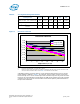
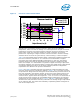
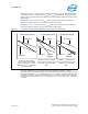
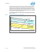
Figure 5 illustrates processor-operating states as the VID level is lowered. The diagram
assumes steady state, maximum current during the transition for ease of illustration.
In this figure, the processor begins in a high-load condition. Upon entering D-VID, the
processor will shift to a low power state and stop executing code (sequence 1 => 2).
After reaching state 2, the processor encounters a brief delay to prepare for low power
operation then re-initiates code, resulting in current draw and a load line IR drop to
state 3. Sequencing from state 3 to 4 is a simplification of the multiple steps from the
original VID load line window to the low-voltage VID window. Transition from state 4 to
state 5 is an example of a load change during normal operation in the low voltage VID
setting. Transition from a low to high VID reference follows the reverse sequence.
During a D-VID transition, V
CC
must always reside above the minimum load line of the
current VID setting (see Figure 5). The load line values of each VID increment are
required to match the slope defined in Table 4. In addition, the voltage tolerance band
and ripple specifications defined in Table 4 and Section Voltage Tolerance Band (TOB)
must be satisfied in this state. To expedite power reduction and processor cooling, the
EmVRD must lower the maximum V
CC
value to reside within the low voltage VID
window within 50 microseconds of the final VID code transmission (see Figure 5). The
EmVRD must respond to a transition from low VID to high VID by regulating the V
CC
output to the range defined by the new VID code within 50 microseconds of the final
code transmission. Note: the minimum VID is not constant among all processors; the
value will vary with frequency and standard VID settings. This results in numerous
possible D-VID states. A simple and direct D-VID validation method is defined at the
end of this section.