
Embedded Voltage Regulator-Down (EmVRD) 11.0 Design Guidelines for Embedded Implementations Supporting PGA478

Embedded Voltage Regulator-Down (EmVRD) 11.0
January 2007 Design Guidelines for Embedded Implementations
13
2.0—EmVRD 11.0
Operating at a low load-line resistance results in higher processor operating
temperature, which can result in damage or a reduced processor life span. Processor
temperature increases from higher functional voltages can lead to operation at low
power states, which may force the platform to induce a reduction in processor
performance. Operating at a higher load-line resistance results in minimum voltage
violations which can result in system lock-up, “blue screening”, or data corruption.
Table 4 lists the EmVRD voltage regulator design configuration intended to support the
Dual-Core Intel Xeon processor LV. It is common for a motherboard to support
processors that require different EmVRD configurations. In this case, the voltage
regulator design must meet the specifications of all processors supported by that
board. For example, if a motherboard is targeted to support this family of processors,
the voltage regulator must have the ability to support the highest power requirements
amongst the twothree processors in this family. Detailed processor configuration
requirements are defined in the processor datasheets.
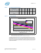
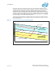
Figure 1 and Table 3 describe minimum and maximum voltage boundaries for each
processor load line design configuration defined in Table 4. V
CCTYP
processor load lines
are provided for design reference. Designers should calibrate the processor load line to
this case (centered in the load line window, at the mean of the tolerance band). The
reader should not assume that processors with similar characteristics will have the
same VID value. Typical values will range from 1.1 V to 1.5 V in 12.5 mV increments. A
single load line chart and figure for each EmVRD design configuration can represent
functionality for each possible VID value. Figure 1 and Table 3 presented as voltage
deviation from VID provide the necessary information to identify voltage requirements
at any reference VID. This avoids the redundancy of publishing tables and figures for
each of the multiple cases.
Figure 2. Processor Load Transient Limits
Processor Load Line
-0.12
-0.10
-0.08
-0.06
-0.04
-0.02
0.00
0.02
0.04
0 5 10 15 20 25 30 35
Output Current, Icc (A)
Vcc minus VID (V)
Vccmax (V)-VID
Vcctyp (V)-VID
Vccmin (V)-VID
Current Step
Vcc Transient Response