MI910/MI910F Intel ® CoreTM 2 Duo/ Celeron GM965 Mini-ITX Motherboard USER’S MANUAL Version 1.
Acknowledgments Award is a registered trademark of Award Software International, Inc. PS/2 is a trademark of International Business Machines Corporation. Intel and Intel® Core 2 Duo and Intel® Celeron processors are registered trademarks of Intel Corporation. Microsoft Windows is a registered trademark of Microsoft Corporation. Winbond is a registered trademark of Winbond Electronics Corporation. All other product names or trademarks are properties of their respective owners.
Table of Contents Introduction .......................................................1 Product Description............................................................. 1 Checklist.............................................................................. 2 MI910 Specifications .......................................................... 3 Board Dimensions ............................................................... 4 Installations .......................................................
IMPORTANT NOTE: When the system boots without the CRT being connected, there will be no image on screen when you insert the CRT/VGA cable. To show the image on screen, the hotkey must be pressed (CTRL-ALT-F1).
INTRODUCTION Introduction Product Description The MI910 Mini ITX board incorporates the Mobile Intel® GM965 Express Chipset for Embedded Computing, consisting of the Intel® GM965 Graphic Memory Controller Hub (GMCH) and Intel® I/O Controller Hub (ICH8-M), an optimized integrated graphics solution with a 533MHz and 800MHz front-side bus. Dimensions of the board are 170mm x 170mm.
INTRODUCTION Checklist Your MI910 package should include the items listed below.
INTRODUCTION MI910 Specifications CPU Supported CPU Voltage System Speed CPU FSB Cache Green /APM CPU Socket Chipset BIOS Memory VGA SDVO (Dual CH) LVDS LCD Panel LAN USB Serial ATA Ports 1394 Parallel IDE Audio LPC I/O Digital IO Keyboard/Mouse Expansion Slots Edge Connector Onboard Header/ Connector Watchdog Timer System Voltage Others Board Size Intel® CoreTM 2 Duo, Intel Celeron mobile processors 0.700V ~ 1.5V (IMVP-6) Up to 2.4GHz or above 533MHz/800MHz FSB 1MB/2MB/4MB APM1.
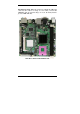
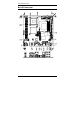
INTRODUCTION [ Board Dimensions 4 MI910 User’s Manual
INSTALLATIONS Installations This section provides information on how to use the jumpers and connectors on the MI910 in order to set up a workable system. The topics covered are: Installing the CPU........................................................................ 6 Installing the Memory.................................................................. 7 Setting the Jumpers ...................................................................... 8 Connectors on MI910 .....................................
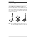
INSTALLATIONS Installing the CPU The MI910 board supports a Socket 478MN (MEROM) processor socket for Intel® CoreTM 2 Duo, Intel® Celeron mobile processors. The processor socket comes with a screw to secure the processor. As shown in the left picture below, loosen the screw first before inserting the processor. Place the processor into the socket by making sure the notch on the corner of the CPU corresponds with the notch on the inside of the socket.
INSTALLATIONS Installing the Memory The Mi910 board supports two DDR2 memory socket for a maximum total memory of 4GB in DDR2 memory type. Installing and Removing Memory Modules To install the DDR2 modules, locate the memory slot on the board and perform the following steps: 1. Hold the DDR2 module so that the key of the DDR2 module aligned with that on the memory slot. 2.
INSTALLATIONS Setting the Jumpers Jumpers are used on MI910 to select various settings and features according to your needs and applications. Contact your supplier if you have doubts about the best configuration for your needs. The following lists the connectors on MI910 and their respective functions. Jumper Locations on MI910........................................................... 9 JP5: LCD Panel Power Selection.................................................. 10 JP9: PCI/PCIE Riser Card Selection .
INSTALLATIONS Jumper Locations on MI910 Jumpers on MI910............................................................................Page JP5: LCD Panel Power Selection ................................................. 10 JP9: PCI/PCIE Riser Card Selection ............................................ 10 JBAT1: Clear CMOS Setting ....................................................... 10 JP8: CompactFlash Slave/Master Selection .................................
INSTALLATIONS JP5: LCD Panel Power Selection JP5 LCD Panel Power 3.
INSTALLATIONS Connectors on MI910 CN1: PS/2 Keyboard and PS/2 Mouse Connectors...................... 14 CN2, CN3: COM1 and VGA Connector...................................... 14 USB_LAN1: 10/100 RJ-45(MI910), GbE RJ45(MI910G) and USB1/2 Ports................................................................................ 15 CN4: 1394 Connector................................................................... 15 J6: SPDIF Out Connector.............................................................
INSTALLATIONS Connector Locations on MI910 12 MI910 User’s Manual
INSTALLATIONS MI910 Solder Side MI910 User’s Manual 13
INSTALLATIONS CN1: PS/2 Keyboard and PS/2 Mouse Connectors PS/2 Mouse PS/2 Keyboard Signal Name Keyboard data N.C. GND 5V Keyboard clock N.C. Keyboard 1 2 3 4 5 6 Mouse 1 2 3 4 5 6 CN2, CN3: COM1 and VGA Connector Signal Name Pin # DCD 1 RXD 2 TXD 3 DTR 4 GND 5 Signal Name Mouse data N.C. GND 5V Mouse clock N.C. [ Pin # Signal Name 6 DSR 7 RTS 8 CTS 9 RI 10 Not Used [[[[ Signal Name Red Blue GND GND N.C. N.C. HSYNC NC 14 Pin # 1 3 5 7 9 11 13 15 Pin # Signal Name 2 Green 4 N.C.
INSTALLATIONS USB_LAN1: 10/100 RJ-45(MI910), 10/100/1000 RJ45(MI910G) and USB1/2 Ports CN4: 1394 Connector J6: SPDIF Out Connector CN5, CN6: GbE RJ-45(MI910F) and USB3/4 Ports CN7: Audio Connector FAN1: System Fan Power Connector FAN1 is a 3-pin header for system fans. The fan must be a 12V (500mA). Pin # 1 2 3 Signal Name Ground +12V Rotation detection FAN2: CPU Fan Power Connector FAN2 is a 3-pin header for the CPU fan. The fan must be a 12V fan.
INSTALLATIONS IDE1: IDE Connector Signal Name Reset IDE Host data 7 Host data 6 Host data 5 Host data 4 Host data 3 Host data 2 Host data 1 Host data 0 Ground DRQ0 Host IOW Host IOR IOCHRDY DACK0 IRQ14 Address 1 Address 0 Chip select 0 Activity Pin # 1 3 5 7 9 11 13 15 17 19 21 23 25 27 29 31 33 35 37 39 Pin # 2 4 6 8 10 12 14 16 18 20 22 24 26 28 30 32 34 36 38 40 Signal Name Ground Host data 8 Host data 9 Host data 10 Host data 11 Host data 12 Host data 13 Host data 14 Host data 15 Protect pin Ground
INSTALLATIONS ATX1: ATX Power Supply Connector 11 1 20 10 Signal Name 3.3V -12V Ground PS-ON Ground Ground Ground -5V +5V +5V Pin # 11 12 13 14 15 16 17 18 19 20 Pin # 1 2 3 4 5 6 7 8 9 10 Signal Name 3.3V 3.3V Ground +5V Ground +5V Ground Power good 5VSB +12V J1 (F_PANEL): System Function Connector J1 provides connectors for system indicators that provide light indication of the computer activities and switches to change the computer status.
INSTALLATIONS Power LED: Pins 11 - 15 Pin # 11 12 13 14 15 Signal Name Power LED No connect Ground No connect Ground ATX Power ON Switch: Pins 7 and 17 This 2-pin connector is an “ATX Power Supply On/Off Switch” on the system that connects to the power switch on the case. When pressed, the power switch will force the system to power on. When pressed again, it will force the system to power off.
INSTALLATIONS F_USB1: USB0/USB1 Connector Signal Name Vcc D0D0+ Ground Pin 1 3 5 7 Pin 2 4 6 8 Signal Name Vcc D1D1+ Ground NC 9 10 Ground JP1, JP2, JP3: RS232/422/485 (COM2) Selection COM1 is fixed for RS-232 use only. COM2 is selectable for RS232, RS-422 and RS-485. The following table describes the jumper settings for COM2 selection.
INSTALLATIONS J2: COM2 Serial Port COM2 Signal Name DCD, Data carrier detect RXD, Receive data TXD, Transmit data DTR, Data terminal ready GND, ground Pin # 1 2 3 4 5 Pin # 6 7 8 9 10 Signal Name DSR, Data set ready RTS, Request to send CTS, Clear to send RI, Ring indicator Not Used J3, J4: LVDS Connectors (1st channel, 2nd channel) The LVDS connectors on board consist of the first channel (J3) and second channel (J4). Signal Name TX0Ground TX15V/3.3V NA TX2Ground TXC5V/3.
INSTALLATIONS J8: Digital I/O Signal Name GND OUT3 OUT2 IN3 IN2 Pin 1 3 5 7 9 Pin 2 4 6 8 10 Signal Name VCC OUT1 OUT0 IN1 IN0 J9: CD-In Pin Header Pin # Signal Name 1 CD Audio R 2 Ground 3 Ground 4 CD Audio L J10: SPI Flash Connector (factory use only) J11: 1394 Connector Signal Name TPA+ TPA+12V GND Pin 1 3 5 7 J12: Front Audio Connector Signal Name Pin # MIC2_L 1 MIC2_R 3 Line2_L 5 Sense 7 Line2_R 9 Pin 2 4 6 8 Signal Name TPB+ TPBNC NC Pin # 2 4 6 8 10 Signal Name Ground Presence# MIC2_ID NC
INSTALLATIONS J14: IrDA Connector Pin # 1 2 3 4 5 Signal Name +5V No connect Ir RX Ground Ir TX J15: Compact Flash Connector PCI1: PCI Slot (supports 2 Master) CON1: SDVO Port Connector 22 Signal Name Pin # Pin # Signal Name +12V +12V +5V 3.
INSTALLATIONS Headers and Connectors on MI910 Daughter Cards ID390 – JP4 LCD Panel Power Selection JP4 Voltage 3.3V 5V ID390 – J1 LCD Backlight Setting Pin # 1 2 3 Signal Name +12V Backlight Enable Ground ID390 – J3 and J2 1st/2nd LVDS Channel Connectors Signal Name TX0Ground TX15V/3.3V TX3TX2Ground TXC5V/3.
INSTALLATIONS ID390C – J4 VGA Connector [[[[ Signal Name +5V Ground N.C. SDA HSYNC VSYNC SCL N.C. 24 Pin # 2 4 6 8 10 12 14 16 Pin # Signal Name 1 RED 3 GREEN 5 BLUE 7 N.C.
INSTALLATIONS ID391 – J2 DVI Connector Signal Name TDC1Ground TLC+5V NC TDC2Ground TDC0NC DDC_SC Pin # 2 4 6 8 10 12 14 16 18 20 Pin # 1 3 5 7 9 11 13 15 17 19 Signal Name TDC1+ Ground TLC+ Ground HPDET TDC2+ Ground TDC0+ NC DDC_SD ID391D – J1, J2 1st/2nd DVI Connectors Signal Name TDC1Ground TLC+5V NC TDC2Ground TDC0NC DDC_SC Pin # 2 4 6 8 10 12 14 16 18 20 Pin # 1 3 5 7 9 11 13 15 17 19 Signal Name TDC1+ Ground TLC+ Ground HPDET TDC2+ Ground TDC0+ NC DDC_SD Remarks: When using dual DVI, the first
INSTALLATIONS This page is intentionally left blank.
BIOS SETUP BIOS Setup This chapter describes the different settings available in the Award BIOS that comes with the board. The topics covered in this chapter are as follows: BIOS Introduction ........................................................................ 28 BIOS Setup................................................................................... 28 Standard CMOS Setup ................................................................. 30 Advanced BIOS Features ..................................
BIOS SETUP BIOS Introduction The Award BIOS (Basic Input/Output System) installed in your computer system’s ROM supports Intel processors. The BIOS provides critical low-level support for a standard device such as disk drives, serial ports and parallel ports. It also adds virus and password protection as well as special support for detailed fine-tuning of the chipset controlling the entire system.
BIOS SETUP Phoenix - AwardBIOS CMOS Setup Utility Standard CMOS Features Advanced BIOS Features Advanced Chipset Features Integrated Peripherals Power Management Setup PnP/PCI Configurations PC Health Status Frequency/Voltage Control Load Fail-Safe Defaults Load Optimized Defaults Set Supervisor Password Set User Password Save & Exit Setup Exit Without Saving ESC : Quit F10 : Save & Exit Setup : Select Item Time, Date, Hard Disk Type… The section below the setup items of the Main Menu displays the con
BIOS SETUP Standard CMOS Setup “Standard CMOS Setup” choice allows you to record some basic hardware configurations in your computer system and set the system clock and error handling. If the motherboard is already installed in a working system, you will not need to select this option. You will need to run the Standard CMOS option, however, if you change your system hardware configurations, the onboard battery fails, or the configuration stored in the CMOS memory was lost or damaged.
BIOS SETUP To set the date, highlight the “Date” field and use the PageUp/ PageDown or +/- keys to set the current time. Time The time format is: Hour : 00 to 23 Minute : 00 to 59 Second : 00 to 59 To set the time, highlight the “Time” field and use the / or +/- keys to set the current time. IDE Channel Master/Slave The onboard PCI IDE connector provides Primary and Secondary channels for connecting up to two IDE hard disks or other IDE devices. Press to configure the hard disk.
BIOS SETUP Video This field selects the type of video display card installed in your system. You can choose the following video display cards: EGA/VGA For EGA, VGA, SEGA, SVGA or PGA monitor adapters. (default) CGA 40 Power up in 40 column mode. CGA 80 Power up in 80 column mode. MONO For Hercules or MDA adapters. Halt On This field determines whether or not the system will halt if an error is detected during power up. No errors The system boot will not be halted for any error that may be detected.
BIOS SETUP Advanced BIOS Features This section allows you to configure and improve your system and allows you to set up some system features according to your preference.
BIOS SETUP Quick Power On Self Test When enabled, this field speeds up the Power On Self Test (POST) after the system is turned on. If it is set to Enabled, BIOS will skip some items. First/Second/Third Boot Device These fields determine the drive that the system searches first for an operating system. The options available include Floppy, LS120, Hard Disk, CDROM, ZIP100, USB-Floppy, USB-ZIP, USB-CDROM, LAN and Disable.
BIOS SETUP Typematic Delay (Msec) When the typematic rate is enabled, this item allows you to set the time interval for displaying the first and second characters. By default, this item is set to 250msec. Security Option This field allows you to limit access to the System and Setup. The default value is Setup. When you select System, the system prompts for the User Password every time you boot up.
BIOS SETUP Advanced Chipset Features This Setup menu controls the configuration of the chipset.
BIOS SETUP On-Chip VGA Setting The fields under the On-Chip VGA Setting and their default settings are: PEG/On Chip VGA Control: Auto On-Chip Frame Buffer Size: 8MB DVMT Mode: DVTM DVMT/Fixed Memory Size: 128MB SDVO Device Setting: (LVDS, DVI, Dual DVI, CRT); Dual LVDS [onboard + ID390] Remarks: Set to LVDS for ID390, Set to CRT for ID390C, Set to DVI for ID391/ID392/ID391D/ID392D.
BIOS SETUP Integrated Peripherals This section sets configurations for your hard disk and other integrated peripherals. The first screen shows three main items for user to select. Once an item selected, a submenu appears. Details follow.
BIOS SETUP Phoenix - AwardBIOS CMOS Setup Utility SuperIO Device POWER ON Function KB Power ON Password Hot Key power ON Onboard Serial Port 1 Onboard Serial Port 2 UART Mode Select RxD, TxD Active IR Transmission Delay UR2 Duplex Mode Use IR Pins PWRON After PWR-Fail BUTTON ONLY Enter Ctrl-F1 3F8/IRQ4 2F8/IRQ3 Normal Hi, Lo Disabled Half IR-Rx2Tx2 Off ITEM HELP Menu Level > IDE HDD Block Mode This field allows your hard disk controller to use the fast block mode to transfer data to and from your hard d
BIOS SETUP On-Chip Serial ATA Setting The fields under the SATA setting includes On-Chip Serial ATA (Auto), PATA IDE Mode (Secondary) and SATA Port (PO, P2 is Primary). AC97 Audio Select This field, by default, is set to Auto. Power ON Function This field is related to how the system is powered on – such as with the use of conventional power button, keyboard or hot keys. The default is BUTTON ONLY.
BIOS SETUP Onboard Serial Port These fields allow you to select the onboard serial ports and their addresses. The default values for these ports are: Serial Port 1 3F8/IRQ4 Serial Port 2 2F8/IRQ3 UART Mode Select This field determines the UART 2 mode in your computer. The default value is Normal. Other options include IrDA and ASKIR. PWRON After PWR-Fail This field sets the system power status whether on or off when power returns to the system from a power failure situation.
BIOS SETUP Power Management Setup Phoenix - AwardBIOS CMOS Setup Utility Power Management Setup ACPI Function Enabled ACPI Suspend RUN VGABIOS if S3 Resume Power Management Video Off Method Video Off In Suspend Suspend Type Modem Use IRQ Suspend Mode HDD Power Down Soft-Off by PWR-BTTN Wake-Up by PCI Card Power On by Ring Resume by Alarm Date (of Month) Alarm Time (hh:mm:ss) Alarm S3(POS) Auto User Define DPMS Yes Stop Grant 3 Disabled Disabled Instant-Off Disabled Disabled Disabled 0 0:0:0 ** Reload G
BIOS SETUP Video Off Method This field defines the Video Off features. There are three options. V/H SYNC + Blank Default setting, blank the screen and turn off vertical and horizontal scanning. DPMS Allows BIOS to control the video display. Blank Screen Writes blanks to the video buffer. Video Off In Suspend When enabled, the video is off in suspend mode. The default setting is Yes. Suspend Type The default setting for the Suspend Type field is Stop Grant.
BIOS SETUP Resume by Alarm This field enables or disables the resumption of the system operation. When enabled, the user is allowed to set the Date and Time. Reload Global Timer Events The HDD, FDD, COM, LPT Ports, and PCI PIRQ are I/O events that can prevent the system from entering a power saving mode or can awaken the system from such a mode. When an I/O device wants to gain the attention of the operating system, it signals this by causing an IRQ to occur.
BIOS SETUP PNP/PCI Configurations This option configures the PCI bus system. All PCI bus systems on the system use INT#, thus all installed PCI cards must be set to this value.
BIOS SETUP PC Health Status This section shows the parameters in determining the PC Health Status. These parameters include temperatures, fan speeds and voltages. Phoenix - AwardBIOS CMOS Setup Utility PC Health Status Shutdown Temperature CPU Warning Temperature Current System Temp Current CPU Temp FAN1 Speed FAN2 Speed Vcore(V) 12 V 1.8V +5V -12V 3.3V VBAT (V) 5VSB(V) 1st Smart Fan Temperature 2st Smart Fan Temperature Disabled Disabled 45°C/113°F 45°C/113°F 5400 RPM 5400 RPM 1.02 V 1.32 V 1.8V 5.
BIOS SETUP Frequency/Voltage Control This section shows the user how to configure the processor frequency. Phoenix - AwardBIOS CMOS Setup Utility Frequency/Voltage Control Auto Detect PCI Clk Disabled Spread Spectrum Modulated Disabled ITEM HELP Menu Level > Auto Detect PCI Clk This field enables or disables the auto detection of the PCI clock. Spread Spectrum Modulated This field sets the value of the spread spectrum. The default setting is Disabled. This field is for CE testing use only.
BIOS SETUP Load Fail-Safe Defaults This option allows you to load the troubleshooting default values permanently stored in the BIOS ROM. These default settings are non-optimal and disable all high-performance features. Load Optimized Defaults This option allows you to load the default values to your system configuration. These default settings are optimal and enable all high performance features. Set Supervisor Password These two options set the system password.
DRIVERS INSTALLATION Drivers Installation This section describes the installation procedures for software and drivers under the Windows 2000 and Windows XP. The software and drivers are included with the motherboard. If you find the items missing, please contact the vendor where you made the purchase. The contents of this section include the following: Intel Chipset Software Installation Utility ................................. 50 VGA Drivers Installation ..................................................
DRIVER INSTALLATION Intel Chipset Software Installation Utility The Intel Chipset Drivers should be installed first before the software drivers to enable Plug & Play INF support for Intel chipset components. Follow the instructions below to complete the installation under Windows 2000/XP. 1. Insert the CD that comes with the board. Click Intel Chipsets and then Intel(R)GM 965Chipset Drivers. 2. Click Intel(R) Chipset Software Installation Utility. 3.
DRIVERS INSTALLATION 4. Click Yes to accept the software license agreement and proceed with the installation process. 5. On Readme Information screen, click Next to continue the installation. 6. The Setup process is now complete. Click Finish to restart the computer and for changes to take effect. When the computer has restarted, the system will be able to find some devices. Restart your computer when prompted.
DRIVER INSTALLATION VGA Drivers Installation To install the VGA drivers, follow the steps below to proceed with the installation. 1. Insert the CD that comes with the motherboard. Click Intel Chipsets and then Intel(R) GM965Chipset Drivers. 2. Click Intel(R) GM965Chipset Family Graphics Driver. 3. When the Welcome screen appears, click Next to continue.
DRIVERS INSTALLATION 4. Click Yes to to agree with the license agreement and continue the installation. 5. Restart the computer as promted and for changes to take effect. IMPORTANT NOTE: When you have restarted the computer, your computer screen will be blank. At this point, press CTRL-ALT-F1 simultaneously, if you are using CRT monitor. If you are using LVDS LCD panel, press CTRL-ALT-F3. If you are using DVI monitor, press CTRL-ALT-F4.
DRIVER INSTALLATION AC97 Codec Audio Driver Installation Follow the steps below to install the Realtek AC97 Codec Audio Drivers. 1. Insert the CD that comes with the motherboard. Click Intel Chipsets and then Intel(R) GM965Chipset Drivers. 2. Click Realtek AC'97 Codec Audio Driver. 3. Click Finish to restart the computer and for changes to take effect. .
DRIVERS INSTALLATION LAN Drivers Installation Follow the steps below to complete the installation of the Intel PRO LAN drivers. 1. Insert the CD that comes with the motherboard. Click Intel Chipsets and then Intel(R) GM965Chipset Drivers, then Intel(R) PRO LAN Network Drivers. 2. Click Install Base Software to continue. 3. When prompted, please to restart the computer for new settings to take effect.
DRIVER INSTALLATION Follow the steps below to install the Marvell Gigabit LAN drivers. 1. Insert the CD that comes with the motherboard. Click LAN Card and then Marvell LAN Controller Driver. 2. Click Next when the InstallShield Wizard welcome screen appears. 3. Click Next to agree with the license agreement. 4. Click Next when the Readme Information screen appears to proceed with the drives installation process. 5. When the Installation is complete, click Finish for the changes to take effect.
APPENDIX Appendix A. I/O Port Address Map Each peripheral device in the system is assigned a set of I/O port addresses which also becomes the identity of the device. The following table lists the I/O port addresses used.
APPENDIX B. Interrupt Request Lines (IRQ) Peripheral devices use interrupt request lines to notify CPU for the service required. The following table shows the IRQ used by the devices on board.
APPENDIX C. Watchdog Timer Configuration The WDT is used to generate a variety of output signals after a user programmable count. The WDT is suitable for use in the prevention of system lock-up, such as when software becomes trapped in a deadlock. Under these sorts of circumstances, the timer will count to zero and the selected outputs will be driven. Under normal circumstance, the user will restart the WDT at regular intervals before the timer counts to zero.
APPENDIX void copyright(void) { printf("\n======== Winbond 83627EHF Watch Timer Tester (AUTO DETECT) ========\n"\ " Usage : W627E_WD reset_time\n"\ " Ex : W627E_WD 3 => reset system after 3 second\n"\ " W627E_WD 0 => disable watch dog timer\n"); } //=========================================================================== void EnableWDT(int interval) { unsigned char bBuf; bBuf = Get_W627EHF_Reg( 0x2D); bBuf &= (!0x01); Set_W627EHF_Reg( 0x2D, bBuf); //Enable WDTO Set_W627EHF_LD( 0x08); Set_W627EHF_Reg( 0
APPENDIX //=========================================================================== // // THIS CODE AND INFORMATION IS PROVIDED "AS IS" WITHOUT WARRANTY OF ANY // KIND, EITHER EXPRESSED OR IMPLIED, INCLUDING BUT NOT LIMITED TO THE // IMPLIED WARRANTIES OF MERCHANTABILITY AND/OR FITNESS FOR A PARTICULAR // PURPOSE. // //=========================================================================== #include "W627EHF.H" #include
APPENDIX //=========================================================================== void Set_W627EHF_Reg( unsigned char REG, unsigned char DATA) { Unlock_W627EHF(); outportb(W627EHF_INDEX_PORT, REG); outportb(W627EHF_DATA_PORT, DATA); Lock_W627EHF(); } //=========================================================================== unsigned char Get_W627EHF_Reg(unsigned char REG) { unsigned char Result; Unlock_W627EHF(); outportb(W627EHF_INDEX_PORT, REG); Result = inportb(W627EHF_DATA_PORT); Lock_W627EHF();