MB935 Socket LGA775 Pentium® 4 Intel® Q35 Chipset Sever Motherboard USER’S MANUAL Version 1.
Acknowledgments Award is a registered trademark of Award Software International, Inc. PS/2 is a trademark of International Business Machines Corporation. Intel and Pentium 4 are registered trademarks of Intel Corporation. Microsoft Windows is a registered trademark of Microsoft Corporation. Winbond is a registered trademark of Winbond Electronics Corporation. All other product names or trademarks are properties of their respective owners.
Table of Contents Introduction ....................................................... 1 Product Description ............................................................. 1 Checklist .............................................................................. 2 Specifications ...................................................................... 3 Board Dimensions ............................................................... 4 Installations .......................................................
The MB935 Motherboard iv MB935 User’s Manual
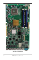
INTRODUCTION Introduction Product Description The MB935 LGA 775 Pentium® 4 motherboard incorporates the Intel Q35 chipset that can utilize a single LGA775 processor of up to 4.0GHz or higher and supports FSB frequency of 800/1066 Mhz/1333Mhz 200MHz (800MT/s), 266MHz (1066MT/s), and 333MHz (1333MT/s) HCLK respectively. The Q35 chipset is designed for use with the Core.2 processor family, including a faster 1333 MHz system bus.
INTRODUCTION Checklist Your MB935 Pentium® 4 motherboard package should include the items listed below: • The MB935 motherboard • This User’s manual • 1 VGA cable • 1 IDE cable • 1 USB cable • 1 PS/2 Keyboard/Mouse cable • 1 SATA cable • 1 Serial-Port cable • 1 CD containing the following: • Chipset Drivers • Flash Memory Utility Reminder: About SATA: When using the legacy operating system, only one controller is available and these ports are SATA port 0,1(CN5, CN6).
INTRODUCTION Specifications Product Name CPU Support MB935 Socket LGA775, Supports the Intel Core 2 Duo and Intel Core2 Quad processors, and Intel Celeron 400 (Conroe-L) Sequence processor. 0.5V~1.6V (VRD 11.0) Up to 3.
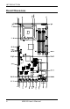
INTRODUCTION Board Dimensions 4 MB935 User’s Manual
INSTALLATIONS Installations This section provides information on how to use the jumpers and connectors on the MB935 in order to set up a workable system. The topics covered are: Installing the CPU ........................................................................ 6 ATX Power Installation ............................................................... 7 Installing the Memory .................................................................. 7 Setting the Jumpers .......................................
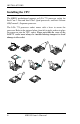
INSTALLATIONS Installing the CPU The MB935 motherboard supports an LGA 775 processor socket for Intel Core 2 Duo and Intel Core2 Quad processors, and Intel Celeron 400(Conroe-L) Sequence processor. The LGA 775 processor socket comes with a lever to secure the processor. Refer to the pictures below, from left to right, on how to place the processor into the CPU socket. Please note that the cover of the LGA775 socket must always be installed during transport to avoid damage to the socket.
INSTALLATIONS ATX Power Installation The system power is provided to the motherboard with the ATX1 and ATX_12V power connectors. ATX1 is a 24-pin power connector and ATX_12V is a 8-pin 12V power connector. The 24-pin power connector can to be connected to a standard 20-pin ATX power connector in a standard ATX power supply (Min. 400watt). Note: The power supply 5VSB voltage must be at least 2A.
INSTALLATIONS Setting the Jumpers Jumpers are used on MB935 to select various settings and features according to your needs and applications. Contact your supplier if you have doubts about the best configuration for your needs. The following lists the connectors on MB935 and their respective functions. Jumper Locations on MB935 ................................................................. 9 JP1, JP2: Watchdog Timer & LAN1/LAN2 Bypass Settings ..............
INSTALLATIONS Jumper Locations on MB935 Jumpers on MB935........................................................................... Page JP1, JP2: Watchdog Timer & LAN1/LAN2 Bypass Settings ............. 10 JP9: Configure and Recovery (Factory use only) ................................ 10 JP16: Clear CMOS Contents ............................................................... 10 JP17: Power ON Setting ......................................................................
INSTALLATIONS JP1, JP2: Watchdog Timer & LAN1/LAN2 Bypass Settings JP1, JP2 Setting JP2 Pin 1-2 & 3-4 Open JP1 Pin 1-2 Closed JP2 Pin 1-2 & 3-4 Open JP1 Pin 2-3 Closed JP2 Pin 1-2 & 3-4 Closed JP1 Pin 1-2 Closed (Default) Function System will bypass LANs upon the time out of watchdog timer. System LANs bypass function controlled by SIO GPIO15. System will reboot upon the time out of watchdog timer.
INSTALLATIONS JP17: Power ON Setting JP17 Setting Pin 1-2 Short/Closed Pin 2-3 Short/Closed MB935 User’s Manual Function Power on by power supply AC on Power on by system button 11
INSTALLATIONS Connectors on MB935 The connectors on MB935 allow you to connect external devices such as keyboard, mouse, hard disk drives, printers… etc. The following table lists the connectors on MB935 and their respective functions. Connector Locations on MB935 .......................................................... 13 ATX1: 24-pin ATX Power Connector................................................. 14 ATX_12V1: ATX 12V Power Connector ...........................................
INSTALLATIONS Connector Locations on MB935 MB935 User’s Manual 13
INSTALLATIONS ATX1: 24-pin ATX Power Connector Signal Name 3.3V -12V Ground PS-ON Ground Ground Ground -5V +5V +5V +5V Ground Pin # 13 14 15 16 17 18 19 20 21 22 23 24 Pin # 1 2 3 4 5 6 7 8 9 10 11 12 Signal Name 3.3V 3.3V Ground +5V Ground +5V Ground Power good 5VSB +12V +12V +3.3V ATX_12V1: ATX 12V Power Connector Signal Name +12V +12V +12V +12V Pin # 5 6 7 8 Pin # 1 2 3 4 Signal Name Ground Ground Ground Ground DIMM1, 2: Channel A DDR2 Socket DIMM1, 2 are the first-channel DDR2 sockets.
INSTALLATIONS FAN4: System Fan Power Connector Pin # 1 2 3 4 Signal Name Ground +12V Rotation detection Control CN1: Slim Type II Compact Flash Connector CN2: COM1 Serial Port CN2 (COM1) is a DB-9 connector.
INSTALLATIONS CN14: Front Side Bridge Board to ID370 Signal Name PWR-SW Reset-SW Speaker VCC GND(PWR LED) HDD LED RELAY LED GND GND GPO0 GPO1 GPO2 GPO3 GPO4 GPO5 GPO6 GPO7 VCC GPIO26 GPIO27 GPIO28 VCC3 Pin # 1 3 5 7 9 11 13 15 17 19 21 23 25 27 29 31 33 35 37 39 41 43 Pin # 2 4 6 8 10 12 14 16 18 20 22 24 26 28 30 32 34 36 38 40 42 44 IDE1: Primary and Secondary IDE Connectors 16 MB935 User’s Manual Signal Name GND GND VCC VCC Pull up to VCC Pull up to VCC Pull up to VCC GND GND GPI0 GPI1 GPI2 GPI3 GP
INSTALLATIONS IDE1 Signal Name Pin # Pin # Signal Name Reset IDE Host data 7 Host data 6 Host data 5 Host data 4 Host data 3 Host data 2 Host data 1 Host data 0 Ground DRQ0 Host IOW Host IOR IOCHRDY DACK0 IRQ14 Address 1 Address 0 Chip select 0 Activity VCC Ground 1 3 5 7 9 11 13 15 17 19 21 23 25 27 29 31 33 35 37 39 41 43 2 4 6 8 10 12 14 16 18 20 22 24 26 28 30 32 34 36 38 40 42 44 Ground Host data 8 Host data 9 Host data 10 Host data 11 Host data 12 Host data 13 Host data 14 Host data 15 Key Gr
BIOS SETUP J3: Keyboard / Mouse Connector J3 is a 10-pin header connector, has functions for both keyboard and mouse. The following table shows the pin assignments of this connector. Signal Name Pin # Pin # Signal Name Protect pin 10 5 N.C.
BIOS SETUP BIOS Setup This chapter describes the different settings available in the Award BIOS that comes with the board. The topics covered in this chapter are as follows: BIOS Introduction ........................................................................ 20 BIOS Setup ................................................................................... 20 Standard CMOS Setup ................................................................. 22 Advanced BIOS Features .................................
BIOS SETUP BIOS Introduction The Award BIOS (Basic Input/Output System) installed in your computer system’s ROM supports Intel processors. The BIOS provides critical low-level support for a standard device such as disk drives, serial ports and parallel ports. It also adds virus and password protection as well as special support for detailed fine-tuning of the chipset controlling the entire system.
BIOS SETUP Phoenix - AwardBIOS CMOS Setup Utility Standard CMOS Features Advanced BIOS Features Advanced Chipset Features Integrated Peripherals Power Management Setup PnP/PCI Configurations PC Health Status Frequency/Voltage Control Load Fail-Safe Defaults Load Optimized Defaults Set Supervisor Password Set User Password Save & Exit Setup Exit Without Saving ESC : Quit F10 : Save & Exit Setup Ç È Æ Å : Select Item Time, Date, Hard Disk Type… The section below the setup items of the Main Menu displays
BIOS SETUP Standard CMOS Setup “Standard CMOS Setup” choice allows you to record some basic hardware configurations in your computer system and set the system clock and error handling. If the motherboard is already installed in a working system, you will not need to select this option. You will need to run the Standard CMOS option, however, if you change your system hardware configurations, the onboard battery fails, or the configuration stored in the CMOS memory was lost or damaged.
BIOS SETUP Time The time format is: Hour : 00 to 23 Minute : 00 to 59 Second : 00 to 59 To set the time, highlight the “Time” field and use the / or +/- keys to set the current time. IDE Channel Master/Slave ICH9 supports 4 Serial ATA connectors; ITE controller support 1 CF and 1 IDE connectors. The onboard Serial ATA connectors provide Primary and Secondary channels for connecting up to four Serial ATA hard disks .
BIOS SETUP Video This field selects the type of video display card installed in your system. You can choose the following video display cards: EGA/VGA For EGA, VGA, SEGA, SVGA or PGA monitor adapters. (default) CGA 40 Power up in 40 column mode. CGA 80 Power up in 80 column mode. MONO For Hercules or MDA adapters. Halt On This field determines whether or not the system will halt if an error is detected during power up. No errors The system boot will not be halted for any error that may be detected.
BIOS SETUP Advanced BIOS Features This section allows you to configure and improve your system and allows you to set up some system features according to your preference.
BIOS SETUP First/Second/Third Boot Device These fields determine the drive that the system searches first for an operating system. Boot Other Device These fields allow the system to search for an OS from other devices other than the ones selected in the First/Second/Third Boot Device. Boot Up NumLock Status This allows you to activate the NumLock function after you power up the system. Gate A20 Option This field allows you to select how Gate A20 is worked.
BIOS SETUP Security Option This field allows you to limit access to the System and Setup. The default value is Setup. When you select System, the system prompts for the User Password every time you boot up. When you select Setup, the system always boots up and prompts for the Supervisor Password only when the Setup utility is called up. APIC Mode APIC stands for Advanced Programmable Interrupt Controller. The default setting is Enabled.
BIOS SETUP Advanced Chipset Features This Setup menu controls the configuration of the chipset.
BIOS SETUP System Memory Frequency This field sets the frequency of the DRAM memory installed. The default setting is Auto. The other settings are DDR667 and DDR800. System BIOS Cacheable The setting of Enabled allows caching of the system BIOS ROM at F000h-FFFFFh, resulting in better system performance. However, if any program writes to this memory area, a system error may result. Memory Hole At 15M-16M In order to improve performance, certain space in memory can be reserved for ISA cards.
BIOS SETUP Integrated Peripherals This section sets configurations for your hard disk and other integrated peripherals.. Details follow.
BIOS SETUP IDE HDD Block Mode This field allows your hard disk controller to use the fast block mode to transfer data to and from your hard disk drive. OnChip Primary/Secondary PCI IDE The integrated peripheral controller contains an IDE interface with support for two IDE channels. Select Enabled to activate each channel separately. IDE Primary/Secondary Master/Slave PIO These fields allow your system hard disk controller to work faster.
BIOS SETUP KB Power ON Password This field allows users to set the password when keyboard power on is the mode of the Power ON function. Hot Key Power ON This field sets certain keys, also known as hot keys, on the keyboard that can be used as a ‘switch’ to power on the system. Onboard Serial Port These fields allow you to select the onboard serial ports and their addresses.
BIOS SETUP Power Management Setup The Power Management Setup allows you to save energy of your system effectively.
BIOS SETUP Video Off Method This field defines the Video Off features. There are three options. V/H SYNC + Blank Default setting, blank the screen and turn off vertical and horizontal scanning. DPMS Allows BIOS to control the video display. Blank Screen Writes blanks to the video buffer. Video Off In Suspend When enabled, the video is off in suspend mode. The default setting is Yes. Suspend Type The default setting for the Suspend Type field is Stop Grant.
BIOS SETUP Resume by Alarm This field enables or disables the resumption of the system operation. When enabled, the user is allowed to set the Date and Time. Reload Global Timer Events The HDD, FDD, COM, LPT Ports, and PCI PIRQ are I/O events that can prevent the system from entering a power saving mode or can awaken the system from such a mode. When an I/O device wants to gain the attention of the operating system, it signals this by causing an IRQ to occur.
BIOS SETUP PNP/PCI Configurations This option configures the PCI bus system. All PCI bus systems on the system use INT#, thus all installed PCI cards must be set to this value.
BIOS SETUP PC Health Status This section shows the parameters in determining the PC Health Status. These parameters include temperatures, fan speeds and voltages. Phoenix - AwardBIOS CMOS Setup Utility PC Health Status Shutdown Temperature CPU Warning Temperature System Temp. CPU Temp. FAN1 Speed FAN2 Speed FAN3 Speed Vcore(V) +12V Vmem -5V +5V -12V 3.3V VBAT 5VSB(V) 1st Smart Fan Temperature Disabled Disabled 45°C/113°F 52°C/125°F 5463 RPM 5463 RPM 5388 RPM 1.02 V 12.03 V 1.89 V -5.33 V 4.94 V -12.0 V 3.
BIOS SETUP Frequency/Voltage Control This section shows the user how to configure the processor frequency. Phoenix - AwardBIOS CMOS Setup Utility Frequency/Voltage Control CPU Clock Ratio Unlock Disabled CPU Clock Ratio Auto Detect PCI Clk Spread Spectrum Modulated 9X Disabled Disabled ITEM HELP Menu Level > Auto Detect PCI Clk This field enables or disables the auto detection of the PCI clock. Spread Spectrum Modulated This field sets the value of the spread spectrum. The default setting is Disabled.
BIOS SETUP Load Fail-Safe Defaults This option allows you to load the troubleshooting default values permanently stored in the BIOS ROM. These default settings are non-optimal and disable all high-performance features. Load Optimized Defaults This option allows you to load the default values to your system configuration. These default settings are optimal and enable all high performance features. Set Supervisor Password These two options set the system password.
BIOS SETUP This page is intentionally left blank.
DRIVERS INSTALLATION Drivers Installation This section describes the installation procedures for software and drivers under the Windows 98SE, Windows ME, Windows 2000 and Windows XP. The software and drivers are included with the motherboard. If you find the items missing, please contact the vendor where you made the purchase. The contents of this section include the following: Intel Chipset Device Software Installation ................................ 42 VGA Drivers Installation ..........................
DRIVER INSTALLATION Intel Chipset Device Software Installation The Intel Chipset Drivers should be installed first before the software drivers to enable Plug & Play INF support for Intel chipset components. Follow the instructions below to complete the installation under Windows 98SE/ME/2000/XP. 1. Insert the CD that comes with the board. Click Intel and then Intel(R) Q35 Chipset Drivers. 2. Click Intel(R) Chipset Software Installation Utility.
DRIVERS INSTALLATION 3. When the Welcome screen appears, click Next to continue. Click Yes to accept the software license agreement and proceed with the installation process.
DRIVER INSTALLATION 5. On Readme Information screen, click Next to continue installation. 6. When Setup is complete, click Finish to complete the setup process.
DRIVERS INSTALLATION VGA Drivers Installation To install the VGA drivers, follow the steps below to proceed with the installation. 1. Insert the CD that comes with the motherboard. Click Intel and then Intel(R) Q35 Chipset Drivers. 2. Click Intel(R) Q35 Chipset Family Graphics Driver.
DRIVER INSTALLATION 3. When the Welcome screen appears, click Next to continue. Click Yes to agree with the license agreement and continue installation.
DRIVERS INSTALLATION 4. Click Next to continue the setup process. Restart the computer as prompted and for changes to take effect.
DRIVER INSTALLATION IDE Controller Drivers Installation Follow the steps below to install IDE Controller Drivers. 1. Insert the CD that comes with the motherboard. Click SCI/SATA Card and then ITE8211 IDE Drivers . When the Welcome screen appears, click Next to continue.
DRIVERS INSTALLATION 4. Select Type as ‘Typical’ and click Next to continue. Restart when promoted and finish the installation process.
DRIVER INSTALLATION Intel PRO LAN Drivers Installation Follow the steps below to complete the installation of the Intel PRO LAN drivers. 1. Insert the CD that comes with the motherboard. Click LAN Card and then Intel(R) PRO 82574L LAN Drivers. 2. Click Install Drivers and Software. When the Welcome screen appears, click Next to continue. 3. Click Next to to agree with the license agreement.
DRIVERS INSTALLATION 4. Click the Drivers checkbox as shown below and click Next to continue installation. Then, click Install to begin the installation. 5. When InstallShield Wizard has completed installation, click Finish.
DRIVER INSTALLATION This page is intentionally left blank.
APPENDIX Appendix A. I/O Port Address Map Each peripheral device in the system is assigned a set of I/O port addresses which also becomes the identity of the device. The following table lists the I/O port addresses used.
APPENDIX B. Interrupt Request Lines (IRQ) Peripheral devices use interrupt request lines to notify CPU for the service required. The following table shows the IRQ used by the devices on board.
APPENDIX C. Watchdog Timer Configuration The WDT is used to generate a variety of output signals after a user programmable count. The WDT is suitable for use in the prevention of system lock-up, such as when software becomes trapped in a deadlock. Under these sort of circumstances, the timer will count to zero and the selected outputs will be driven. Under normal circumstance, the user will restart the WDT at regular intervals before the timer counts to zero.
APPENDIX mov cl, 0F5h call Read_Reg and al, NOT 08h call Write_Reg ;set count mode as second pop ax mov cl, 0F6h call Write_Reg ;set watchdog timer mov al, 01h mov cl, 30h call Write_Reg ;watchdog enabled call Lock_Chip ret Enable_And_Set_Watchdog Endp ;[]=============================================== ; Name : Disable_Watchdog ; IN : None ; OUT : None ;[]=============================================== Disable_Watchdog Proc Near call Unlock_Chip mov cl, 07h mov al, 08h call Write_Reg ;switch to LD8
APPENDIX ; Name : Unlock_Chip ; IN : None ; OUT : None ;[]=============================================== Unlock_Chip Proc Near Mov dx, 4Eh mov al, 87h out dx, al out dx, al ret Unlock_Chip Endp ;[]================================================ ; Name : Lock_Chip ; IN : None ; OUT : None ;[]================================================ Unlock_Chip Proc Near mov dx, 4Eh mov al, 0AAh out dx, al ret Unlock_Chip Endp ;[]================================================ ; Name : Write_Reg ; IN : CL - regist
APPENDIX ; Name : Read_Reg ; IN : CL - register index ; OUT : AL - Value to read ;[]================================================= == Read_Reg Proc Near Mov al, cl mov dx, 4Eh out dx, al inc dx in al, dx ret Read_Reg Endp ;[]================================================ 58 MB935 User’s Manual
APPENDIX D. Digital I/O Sample Code Filename: W627hf.h //===================================================================== // // THIS CODE AND INFORMATION IS PROVIDED "AS IS" WITHOUT WARRANTY OF ANY // KIND, EITHER EXPRESSED OR IMPLIED, INCLUDING BUT NOT LIMITED TO THE // IMPLIED WARRANTIES OF MERCHANTABILITY AND/OR FITNESS FOR A PARTICULAR // PURPOSE.
APPENDIX Filename: W627hf.cpp //===================================================================== // // THIS CODE AND INFORMATION IS PROVIDED "AS IS" WITHOUT WARRANTY OF ANY // KIND, EITHER EXPRESSED OR IMPLIED, INCLUDING BUT NOT LIMITED TO THE // IMPLIED WARRANTIES OF MERCHANTABILITY AND/OR FITNESS FOR A PARTICULAR // PURPOSE. // //===================================================================== #include "W627HF.H" #include
APPENDIX //===================================================================== // THIS CODE AND INFORMATION IS PROVIDED "AS IS" WITHOUT WARRANTY OF ANY // KIND, EITHER EXPRESSED OR IMPLIED, INCLUDING BUT NOT LIMITED TO THE // IMPLIED WARRANTIES OF MERCHANTABILITY AND/OR FITNESS FOR A PARTICULAR // PURPOSE. //===================================================================== #include #include #include #include #include "W627HF.
APPENDIX This page is intentionally left blank.