MB884 Socket LGA775 Pentium® 4 Intel® 915G Chipset Industrial Motherboard USER’S MANUAL Version 1.
Acknowledgments Award is a registered trademark of Award Software International, Inc. PS/2 is a trademark of International Business Machines Corporation. Intel and Pentium 4 are registered trademarks of Intel Corporation. Microsoft Windows is a registered trademark of Microsoft Corporation. Winbond is a registered trademark of Winbond Electronics Corporation. All other product names or trademarks are properties of their respective owners.
Table of Contents Introduction .......................................................1 Checklist.............................................................................. 1 Product Description............................................................. 2 MB884 Specifications ......................................................... 3 Board Dimensions ............................................................... 4 Installations .......................................................
This page is intentionally left blank.
INTRODUCTION Introduction Checklist Your MB884 Pentium® 4 motherboard package should include the items listed below: • The MB884 motherboard • This User’s Manual • 1 Back I/O shield • 1 IDE Cable • 1 Floppy Cable • 1 SATA Cable • Optional 3 SATA Cables • Optional Serial Port Cable • 1 CD containing the following: • Chipset Drivers • Flash Memory Utility MB884 User’s Manual 1
INSTALLATIONS Product Description The MB884 LGA 775 Pentium® 4 motherboard incorporates the Intel 915G chipset that can utilize a single LGA775 processor of up to 4.0GHz or higher and supports FSB frequency of 533/800Mhz (133MHz, and 200MHz HCLK respectively). The 915G chipset is designed for use with the Pentium® 4 processor with 1M Level 2 (CPU integrated) cache. The integrated MCH component provides the CPU interface, DDR interface, Hub Interface and PCI Express graphics interface.
INTRODUCTION MB884 Specifications Form Factor CPU Type CPU Voltage CPU FSB CPU FSB Green / APM CPU Socket Chipset BIOS Cache VGA Gigabit LAN Audio Memory Parallel IDE Serial ATA Ports USB LPC I/O RTC Edge Connector Onboard Header / Connector Expansion Slots Power Connector Watchdog Timer System Voltage Other Function Board Size Micro ATX Intel Pentium 4 0.8375V~1.6V (VRD 10.1) 800MHz Up to 3.8+ GHz APM1.
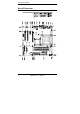
INSTALLATIONS Board Dimensions 4 MB884 User’s Manual
INSTALLATIONS Installations This section provides information on how to use the jumpers and connectors on the MB884 in order to set up a workable system. The topics covered are: Installing the CPU........................................................................ 6 ATX Power Installation ............................................................... 7 Installing the Memory.................................................................. 7 Setting the Jumpers .........................................
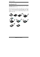
INSTALLATIONS Installing the CPU The MB884 motherboard supports an LGA 775 processor socket for Intel® Pentium® 4 processors. The LGA 775 processor socket comes with a lever to secure the processor. Refer to the pictures below, from left to right, on how to place the processor into the CPU socket. Please note that the cover of the LGA775 socket must always be installed during transport to avoid damage to the socket.
INSTALLATIONS ATX Power Installation The system power is provided to the motherboard with the ATX1 and ATX_12V power connectors. ATX1 is a 24-pin power connector and ATX_12V is a 4-pin 12V power connector. The 24-pin power connector can to be connected to a standard 20-pin ATX power connector in a standard ATX power supply (Min. 400watt). Note: The power supply 5VSB voltage must be at least 2A.
INSTALLATIONS Setting the Jumpers Jumpers are used on MB884 to select various settings and features according to your needs and applications. Contact your supplier if you have doubts about the best configuration for your needs. The following lists the connectors on MB884 and their respective functions. Jumper Locations on MB884.......................................................... 9 JP1: COM2 RS232 +5V/+12V Power Setting.............................. 10 JP2: COM1 RS232 +5V/+12V Power Setting...........
INSTALLATIONS Jumper Locations on MB884 Jumper Locations on MB884 ...........................................................Page JP1: COM2 RS232 +5V/+12V Power Setting .................................... 10 JP2: COM1 RS232 +5V/+12V Power Setting .................................... 10 JP3: RS232/422/485 (COM2) Selection.............................................. 10 JP5: Clear CMOS Contents .................................................................
INSTALLATIONS JP1: COM2 RS232 +5V/+12V Power Setting JP1 Setting Pin 1-2 Short/Closed Pin 3-4 Short/Closed Pin 5-6 Short/Closed Function +12V Normal +5V JP2: COM1 RS232 +5V/+12V Power Setting JP2 Setting Pin 1-2 Short/Closed Pin 3-4 Short/Closed Pin 5-6 Short/Closed Function +12V Normal +5V JP3: RS232/422/485 (COM2) Selection COM1 is fixed for RS-232 use only. JP3, COM2 is selectable for RS232, RS-422 and RS-485. The following table describes the jumper settings for COM2 selection.
INSTALLATIONS JP5: Clear CMOS Contents Use JP5, a 3-pin header, to clear the CMOS contents. Note that the ATX-power connector should be disconnected from the motherboard before clearing CMOS.
INSTALLATIONS [ Connectors on MB884 The connectors on MB884 allows you to connect external devices such as keyboard, floppy disk drives, hard disk drives, printers, etc. The following table lists the connectors on MB884 and their respective functions. Connector Locations on MB884................................................... 13 ATX1: ATX Power Supply Connector......................................... 14 ATX_12V: ATX 12V Power Connector ......................................
INSTALLATIONS Connectors on MB884 .......................................................................................................................................Page ATX1: ATX Power Supply Connector ..................................................................................................................14 ATX_12V: ATX 12V Power Connector ...............................................................................................................14 DIMM1: Channel A DDR Socket.............
INSTALLATIONS ATX1: ATX Power Supply Connector Signal Name Pin # Pin # 3.3V 13 1 -12V 14 2 Ground 15 3 PS-ON 16 4 Ground 17 5 Ground 18 6 Ground 19 7 -5V 20 8 +5V 21 9 +5V 22 10 +5V 23 11 Ground 24 12 Signal Name 3.3V 3.3V Ground +5V Ground +5V Ground Power good 5VSB +12V +12V +3.3V ATX1 is a 24-pin ATX power supply connector.
INSTALLATIONS CN1: PS/2 Keyboard and PS/2 Mouse Connectors PS/2 Mouse PS/2 Keyboard Signal Name Keyboard data N.C. GND 5V Keyboard clock N.C. Keyboard 1 2 3 4 5 6 Mouse 1 2 3 4 5 6 Signal Name Mouse data N.C. GND 5V Mouse clock N.C. CN2: 4-port USB Connector CN2 is a USB connector consisting of four ports stacked vertically. CN2 Pin 1 2 3 4 Signal Name Ground USB+ USBVcc CN3, JP2: COM1/COM2 Serial Ports CN3 (COM1) is a DB-9 connector, while JP2 is a COM2 pin-header connector.
INSTALLATIONS COM2 is jumper selectable for RS-232, RS-422 and RS-485. Pin # RS-232 1 2 3 4 5 6 7 8 9 10 DCD RX TX DTR Ground DSR RTS CTS RI NC Signal Name R2-422 RS-485 TXTX+ RX+ RXGround RTSRTS+ CTS+ CTSNC DATADATA+ NC NC Ground NC NC NC NC NC CN4: Parallel Port Connector CN4 is a DB-25 external connector situated on top of the VGA and serial ports.
INSTALLATIONS CN5: VGA CRT Connector CN5 is a DB-15 VGA connector located beside the COM1 port. The following table shows the pin-out assignments of this connector. Signal Name Red Blue GND GND N.C. N.C. HSYNC NC Pin # 1 3 5 7 9 11 13 15 Pin # Signal Name 2 Green 4 N.C. 6 GND 8 GND 10 GND 12 N.C. 14 VSYNC CN6: DUAL LAN RJ45 Connectors CN6 consists of two RJ-45 connectors that are used in conjunction with the Marvell 88E8053 PCI Express Gigabit LAN single controllers.
INSTALLATIONS J1: Digital I/O Connector (4 in, 4 out) This 10-pin Digital I/O connector supports TTL levels and is used to control external devices requiring ON/OFF circuitry. Signal Name Ground Out3 Out2 IN3 IN2 Pin # 1 3 5 7 9 Pin # 2 4 6 8 10 Signal Name +5V Out1 Out0 IN1 IN0 J3: IrDA Connector Pin # 1 2 3 4 5 Signal Name +5V No connect Ir RX Ground Ir TX J4: USB Connector The following table shows the pin outs of the USB pin header.
INSTALLATIONS J10: Wake On LAN Connector J10 is a 3-pin header for the Wake On LAN function on the motherboard. The following table shows the pin out assignments of this connector. Wake On LAN will function properly only with an ATX power supply with 5VSB that has 1A. Pin # Signal Name 1 +5VSB 2 Ground 3 LAN Wakeup J13: System Function Connector J13 provides connectors for system indicators that provide light indication of the computer activities and switches to change the computer status.
INSTALLATIONS Power LED: Pins 11 - 13 The power LED indicates the status of the main power switch. Pin # 11 12 13 Signal Name Power LED No connect Ground Keyboard Locked: Pin 14-15 To use keyboard lock, set pin14/15 to short/closed Pin # Signal Name 14 Keyboard lock 15 Ground ATX Power ON Switch: Pins 7 and 17 This 2-pin connector is an “ATX Power Supply On/Off Switch” on the system that connects to the power switch on the case. When pressed, the power switch will force the system to power on.
INSTALLATIONS Hard Disk Drive LED Connector: Pins 10 and 20 This connector connects to the hard drive activity LED on control panel. This LED will flash when the HDD is being accessed.
INSTALLATIONS FDD1: Floppy Drive Connector FDD1 Signal Name Ground Ground Ground Ground Ground Ground Ground Ground Ground Ground Ground Ground Ground Ground Ground Ground Ground Pin # 1 3 5 7 9 11 13 15 17 19 21 23 25 27 29 31 33 Pin # 2 4 6 8 10 12 14 16 18 20 22 24 26 28 30 32 34 Signal Name RM/LC No connect No connect Index Motor enable 0 Drive select 1 Drive select 0 Motor enable 1 Direction Step Write data Write gate Track 00 Write protect Read data Side 1 select Diskette change IDE1: Primary I
INSTALLATIONS LED1: LED for CPU Over-Voltage Protection This red LED shall light to indicate that the CPU voltage has surged and reached the default voltage protection value (2V). In such a case, the system will shut down automatically. LED3: Power On LED This green LED will light constantly when the power is on to indicate that the 5VSB status has switched to 5V power. LED5: Power Off LED This Red LED will light constantly during a power-off status to indicate 5VSB status.
INSTALLATIONS Watchdog Timer Configuration The WDT is used to generate a variety of output signals after a user programmable count. The WDT is suitable for use in the prevention of system lock-up, such as when software becomes trapped in a deadlock. Under these sort of circumstances, the timer will count to zero and the selected outputs will be driven. Under normal circumstance, the user will restart the WDT at regular intervals before the timer counts to zero.
INSTALLATIONS mov al, 01h mov cl, 30h call Write_Reg ;watchdog enabled call Lock_Chip ret Enable_And_Set_Watchdog Endp ;[]=============================================== ; Name : Disable_Watchdog ; IN : None ; OUT : None ;[]=============================================== Disable_Watchdog Proc Near call Unlock_Chip mov cl, 07h mov al, 08h call Write_Reg ;switch to LD8 xor al, al mov cl, 0F6h call Write_Reg ;clear watchdog timer xor al, al mov cl, 30h call Write_Reg ;watchdog disabled call Lock_Chip
INSTALLATIONS ;[]================================================ Unlock_Chip Proc Near mov dx, 4Eh mov al, 0AAh out dx, al ret Unlock_Chip Endp ;[]================================================ ; Name : Write_Reg ; IN : CL - register index ; AL - Value to write ; OUT : None ;[]================================================ Write_Reg Proc Near push ax mov dx, 4Eh mov al,cl out dx,al pop ax inc dx out dx,al ret Write_Reg Endp ;[]================================================ ; Name : Read_Reg ; IN : C
INSTALLATIONS Digital I/O Sample Code Filename: W627hf.h //===================================================================== // // THIS CODE AND INFORMATION IS PROVIDED "AS IS" WITHOUT WARRANTY OF ANY // KIND, EITHER EXPRESSED OR IMPLIED, INCLUDING BUT NOT LIMITED TO THE // IMPLIED WARRANTIES OF MERCHANTABILITY AND/OR FITNESS FOR A PARTICULAR // PURPOSE.
INSTALLATIONS Filename: W627hf.cpp //===================================================================== // // THIS CODE AND INFORMATION IS PROVIDED "AS IS" WITHOUT WARRANTY OF ANY // KIND, EITHER EXPRESSED OR IMPLIED, INCLUDING BUT NOT LIMITED TO THE // IMPLIED WARRANTIES OF MERCHANTABILITY AND/OR FITNESS FOR A PARTICULAR // PURPOSE. // //===================================================================== #include "W627HF.H" #include
INSTALLATIONS //===================================================================== // // THIS CODE AND INFORMATION IS PROVIDED "AS IS" WITHOUT WARRANTY OF ANY // KIND, EITHER EXPRESSED OR IMPLIED, INCLUDING BUT NOT LIMITED TO THE // IMPLIED WARRANTIES OF MERCHANTABILITY AND/OR FITNESS FOR A PARTICULAR // PURPOSE. // //===================================================================== #include #include #include #include #include "W627HF.
BIOS SETUP BIOS Setup This chapter describes the different settings available in the Award BIOS that comes with the motherboard. The topics covered in this chapter are as follows: BIOS Introduction ........................................................................ 31 BIOS Setup ................................................................................... 31 Standard CMOS Setup.................................................................. 33 Advanced BIOS Features ...........................
BIOS SETUP BIOS Introduction The Award BIOS (Basic Input/Output System) installed in your computer system’s ROM supports Intel® Pentium® 4 processors. The BIOS provides critical low-level support for a standard device such as disk drives, serial ports and parallel ports. It also adds virus and password protection as well as special support for detailed fine-tuning of the chipset controlling the entire system.
BIOS SETUP Phoenix - AwardBIOS CMOS Setup Utility Standard CMOS Features Advanced BIOS Features Advanced Chipset Features Integrated Peripherals Power Management Setup PnP/PCI Configurations PC Health Status Frequency/Voltage Control Load Fail-Safe Defaults Load Optimized Defaults Set Supervisor Password Set User Password Save & Exit Setup Exit Without Saving ESC : Quit F10 : Save & Exit Setup Ç È Æ Å : Select Item Time, Date, Hard Disk Type… The section below the setup items of the Main Menu display
BIOS SETUP Standard CMOS Setup “Standard CMOS Setup” choice allows you to record some basic hardware configurations in your computer system and set the system clock and error handling. If the board is already installed in a working system, you will not need to select this option. You will need to run the Standard CMOS option, however, if you change your system hardware configurations, the onboard battery fails, or the configuration stored in the CMOS memory was lost or damaged.
BIOS SETUP Time The time format is: Hour : 00 to 23 Minute : 00 to 59 Second : 00 to 59 To set the time, highlight the “Time” field and use the / or +/- keys to set the current time. IDE Primary HDDs / IDE Secondary HDDs The onboard PCI IDE connectors provide Primary and Secondary channels for connecting up to four IDE hard disks or other IDE devices. Each channel can support up to two hard disks; the first is the “Master” and the second is the “Slave”.
BIOS SETUP Video This field selects the type of video display card installed in your system. You can choose the following video display cards: EGA/VGA For EGA, VGA, SEGA, SVGA or PGA monitor adapters. (default) CGA 40 Power up in 40 column mode. CGA 80 Power up in 80 column mode. MONO For Hercules or MDA adapters. Halt On This field determines whether or not the system will halt if an error is detected during power up. No errors The system boot will not be halted for any error that may be detected.
BIOS SETUP Advanced BIOS Features This section allows you to configure and improve your system and allows you to set up some system features according to your preference.
BIOS SETUP This item allows you to set the priority for hard disk boot. When you press enter, the selections shows the current hard disks used in your system as well as the “Bootable Add-in Card” that is relevant to other boot sources media such as SCSI cards and LAN cards. Virus Warning This item protects the boot sector and partition table of your hard disk against accidental modifications. If an attempt is made, the BIOS will halt the system and display a warning message.
BIOS SETUP Swap Floppy Drive This item allows you to determine whether or not to enable Swap Floppy Drive. When enabled, the BIOS swaps floppy drive assignments so that Drive A becomes Drive B, and Drive B becomes Drive A. By default, this field is set to Disabled. Boot Up Floppy Seek This feature controls whether the BIOS checks for a floppy drive while booting up. If it cannot detect one (either due to improper configuration or its absence), it will flash an error message.
BIOS SETUP APIC Mode APIC stands for Advanced Programmable Interrupt Controller. The default setting is Enabled. MPS Version Control for OS This option is specifies the MPS (Multiprocessor Specification) version for your operating system. MPS version 1.4 added extended configuration tables to improve support for multiple PCI bus configurations and improve future expandability. The default setting is 1.4.
BIOS SETUP Advanced Chipset Features This Setup menu controls the configuration of the chipset. Phoenix - AwardBIOS CMOS Setup Utility Advanced Chipset Features DRAM Timing Selectable CAS Latency Time DRAM RAS# to CAS# Delay DRAM RAS# Precharge Precharge dealy (tRAS) System Memory Frequency SLP_S4# Assertion Width System BIOS Cacheable Video BIOS Cacheable Memory Hole At 15M-16M PCI Express Root Port Func By SPD 2.5 3 3 8 400MHz 1 to 2 Sec.
BIOS SETUP DRAM RAS# to CAS# Delay This option allows you to insert a delay between the RAS (Row Address Strobe) and CAS (Column Address Strobe) signals. This delay occurs when the SDRAM is written to, read from or refreshed. Reducing the delay improves the performance of the SDRAM. DRAM RAS# Precharge This option sets the number of cycles required for the RAS to accumulate its charge before the SDRAM refreshes. The default setting for the Active to Precharge Delay is 3.
BIOS SETUP PCI-E Compliancy Mode The default setting is Auto. Another mode is v1.0. PEG/OnChip VGA Control The default setting is Auto. On-Chip Video Memory Size Use this field to select On-Chip Frame Buffer Size, Fixed Memory Size and DVMT Memory Size. Total Graphics Memory can be set as 64MB, 128MB or 224MB. On-Chip Frame Buffer Size The On-Chip Frame Buffer Size can be set us 1MB, 8MB or 16MB. This memory is shared with the system memory.
BIOS SETUP Integrated Peripherals Phoenix - AwardBIOS CMOS Setup Utility Integrated Peripherals OnChip IDE Device Onboard Device SuperIO Device Onboard Lan Boot ROM Press Enter Press Enter Press Enter Disabled IDE HDD Block Mode IDE DMA transfer access On-Chip Primary PCI IDE IDE Primary Master PIO IDE Primary Slave PIO IDE Primary Master UDMA IDE Primary Slave UDMA On-Chip Secondary PCI IDE IDE Secondary Master PIO IDE Secondary Slave PIO IDE Secondary Master UDMA IDE Secondary Slave UDMA Enabled Enabl
BIOS SETUP Onboard LAN Boot ROM This field allows you to enable the on board LAN boot ROM. By default, this option is disabled. IDE HDD Block Mode This field allows your hard disk controller to use the fast block mode to transfer data to and from your hard disk drive. IDE DMA Transfer Access Use this field to enable or disable IDE DMA transfer access. OnChip Primary/Secondary PCI IDE The integrated peripheral controller contains an IDE interface with support for two IDE channels.
BIOS SETUP SATA Port This feature allows users to view the SATA port as primary or secondary channel. USB Controller The options for this field are Enabled and Disabled. By default, this field is set to Enabled. USB 2.0 Controller The options for this field are Enabled and Disabled. By default, this field is set to Enabled. In order to use USB 2.0, necessary OS drivers must be installed first. USB Keyboard Support The options for this field are Enabled and Disabled.
BIOS SETUP Onboard FDC Controller Select Enabled if your system has a floppy disk controller (FDC) installed on the board and you wish to use it. If you install an add-in FDC or the system has no floppy drive, select Disabled in this field. This option allows you to select the onboard FDD port. Onboard Serial/Parallel Port These fields allow you to select the onboard serial and parallel ports and their addresses.
BIOS SETUP Power Management Setup The Power Management Setup allows you to save energy of your system effectively.
BIOS SETUP Video Off In Suspend When enabled, the video is off in suspend mode. Suspend Type The default setting for the Suspend Type field is Stop Grant. Modem Use IRQ This field sets the IRQ used by the Modem. By default, the setting is 3. Suspend Mode When enabled, and after the set time of system inactivity, all devices except the CPU will be shut off.
BIOS SETUP PNP/PCI Configurations This option configures the PCI bus system. All PCI bus systems on the system use INT#, thus all installed PCI cards must be set to this value.
BIOS SETUP PC Health Status This section shows the parameters in determining the PC Health Status. These parameters include temperatures, fan speeds and voltages. Phoenix - AwardBIOS CMOS Setup Utility PC Health Status CPU Warning Temperature System Temp CPU Temp CPU FAN Speed (CPU_FAN1/2) System FAN Speed (FAN1) System FAN Speed (FAN2) Vcore(V) +3.3V +5 V +12 V -12 V VBAT (V) 5VSB (V) Shutdown Temperature CPU Fan Failure Warning Sys. Fan Failure Warning Aux.
BIOS SETUP Frequency/Voltage Control This section shows the user how to configure the processor frequency. Phoenix - AwardBIOS CMOS Setup Utility Frequency/Voltage Control CPU Clock Ratio Auto Detect PCI Clk 14X Disabled Spread Spectrum Disabled ITEM HELP Menu Level CPU Clock Ratio The CPU Ratio, also known as the CPU bus speed multiplier, can be configured through this field. This field will only appear if your CPU allows changes in the CPU clock ratio, such as in the case of engineering-sample CPUs.
BIOS SETUP Load Fail-Safe Defaults This option allows you to load the troubleshooting default values permanently stored in the BIOS ROM. These default settings are non-optimal and disable all high-performance features. Load Setup Defaults This option allows you to load the default values to your system configuration. These default settings are optimal and enable all high performance features. Set Supervisor/User Password These two options set the system password.
DRIVERS INSTALLATION Drivers Installation This section describes the installation procedures for software and drivers under the Windows 2000 and Windows XP. The software and drivers are included with the board. If you find the items missing, please contact the vendor where you made the purchase. The contents of this section include the following: Intel 915G Chipset Software Intallation Utility ......................... 54 Intel 915G Chipset Graphics Driver ..........................................
DRIVERS INSTALLATION Intel 915G Chipset Software Intallation Utility The Intel 915G Chipset Drivers should be installed first before the software drivers to enable Plug & Play INF support for Intel chipset components. Follow the instructions below to complete the installation under Windows 2000/XP. (Before installed Intel Chipset Software Intallation Utility,Please update your system to Windows 2000 SP4 or Windows XP SP1A) 1. Insert the CD that comes with the board and the screen below would appear.
DRIVERS INSTALLATION Intel 915G Chipset Graphics Driver The Intel 915G Chipset Family Graphics Drivers come in the CD with the motherboard. Follow the instructions below to complete the installation under Windows 2000/XP. 1. Insert the CD that comes with the board and the screen below would appear. Click Intel 915G Chipset Family Graphics Driver. 2. When the Welcome screen appears, click Next to continue. 3. Click Yes to accept the software license agreement and proceed with the installation process. 4.
DRIVERS INSTALLATION Realtek AC97 Codec Audio Driver Installation Follow the steps below to install the Realtek AC97 Codec Audio Drivers. 1. Insert the CD that comes with the board and the screen below would appear. Click Realtek AC97 Codec Audio Drivers to start the drivers installation. 2. Click Finish to restart the computer and for changes to take effect.
DRIVERS INSTALLATION Marvell 88E8053 LAN Drivers Installation Follow the steps below to start installing the Marvell 88E8053 PCI Express Gigabit LAN drivers. 1. Insert the CD that comes with the board. In the initial screen, click on LAN Card on the left side. 2. When the Welcome screen appears, click Next to start the drivers instalation. 3. Click Finish to complete the setup and for changes to take effect.
DRIVERS INSTALLATION This page is intentionally left blank.
APPENDIX Appendix A. I/O Port Address Map Each peripheral device in the system is assigned a set of I/O port addresses that also becomes the identity of the device. The following table lists the I/O port addresses used.
APPENDIX B. Interrupt Request Lines (IRQ) Peripheral devices use interrupt request lines to notify CPU for the service required. The following table shows the IRQ used by the devices on board.