MB875 Intel® 852GM Chipset Custom Motherboard for 1U Rackmount USER’S MANUAL Version 1.
Acknowledgments Award is a registered trademark of Award Software International, Inc. PS/2 is a trademark of International Business Machines Corporation. Intel and Pentium M are registered trademarks of Intel Corporation. Microsoft Windows is a registered trademark of Microsoft Corporation. Winbond is a registered trademark of Winbond Electronics Corporation. All other product names or trademarks are properties of their respective owners.
Table of Contents Introduction ....................................................... 1 Product Description ............................................................. 1 Checklist .............................................................................. 2 MB875 Specifications ......................................................... 3 Board Dimensions ............................................................... 4 Installations .......................................................
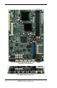
The MB875 Motherboard The MB875 Edge Connectors iv MB890 User’s Manual
INTRODUCTION Introduction Product Description The MB875 is a versatile motherboard with four Gigabit Ethernets that is designed for SOHO network security applications. Optimized for network performance, this scalable platform is based on the Intel(R) 852GM chipset and supports Intel(R) Pentium(R) M / Celeron(R) M processors of up to 2.0GHz speeds with front size bus of 400MHz. System memory can support up to 2GB of DDR266 DIMM modules.
INTRODUCTION Checklist Your MB875 package should include the items listed below.
INTRODUCTION MB875 Specifications [ CPU Type CPU Voltage CPU Speed CPU FSB Cache CPU Socket Chipset Green /APM BIOS Memory VGA LAN USB SATA IDE Interface LPC I/O RTC/CMOS Edge Connectors / LED / Button @front side On Board Connectors / Headers Expansion Power Connector Dimensions Intel ULV Celeron M CPU or Intel Pentium M CPU 0.700V ~ 1.708V 600MHz 400MHz 512K Level 2 (CPU integrated) BGA on board or socket 479 Intel 852GM Chipset: GMCH: 852GM 732-pin mFCBGA ICH4: 82801DB 421-pin BGA, APM1.
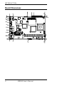
INTRODUCTION Board Dimensions 4 MB890 User’s Manual
INSTALLATIONS Installations This section provides information on how to use the jumpers and connectors on the MB875 in order to set up a workable system. The topics covered are: Installing the CPU ........................................................................ 6 Installing the Memory .................................................................. 7 Setting the Jumpers ...................................................................... 8 Connectors on MB875 ...................................
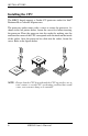
INSTALLATIONS Installing the CPU The MB875 board supports a Socket 479 processor socket for Intel® Pentium® M or Celeron® M processors. The processor socket comes with a screw to secure the processor. As shown in the left picture below, loosen the screw first before inserting the processor. Place the processor into the socket by making sure the notch on the corner of the CPU corresponds with the notch on the inside of the socket. Once the processor has slide into the socket, fasten the screw.
INSTALLATIONS Installing the Memory The MB875 board supports one DDR memory sockets for a maximum total memory of 1GB in DDR memory type. The memory module capacities supported are 128MB, 256MB, 512MB and 1GB. The following table lists the supported DDR DIMM configurations. Intel® 852GM supports configurations defined in the JEDEC DDR DIMM specification only. Non-JEDEC standard DIMMs such as double-sided x16 DDR SDRAM DIMMs are not supported.
INSTALLATIONS Setting the Jumpers Jumpers are used on MB875 to select various settings and features according to your needs and applications. Contact your supplier if you have doubts about the best configuration for your needs. The following lists the connectors on MB875 and their respective functions. Jumper Locations on MB875.......................................................... 9 JP1: CPU Host Clock.................................................................... 10 JP2: Power Mode Setting.......
INSTALLATIONS Jumper Locations on MB875 Jumpers on MB875........................................................................... Page JP1: Clear CMOS Contents ................................................................. 10 JP2: Watchdog Timer Settings ............................................................ 10 JP4: Compact Flash Slave/Master ....................................................... 10 JP5: Processor Operating Frequency ...................................................
INSTALLATIONS JP1: Clear CMOS Contents Use JP1 to clear the CMOS contents. Note that the ATX-power connector should be disconnected from the board before clearing CMOS. JP1 Setting Function Pin 1-2 Short/Closed Normal Pin 2-3 Short/Closed Clear CMOS JP2: Watchdog Timer Settings JP2 Setting Pin 1-2 & 3-4 Short Ethernet default: Eth0 & Eth1 None Bypass. System will bypass LANs upon the timeout of Watchdog timer Ethernet default: Eth0 & Eth1 Bypass mode.
INSTALLATIONS JP5: Processor Operating Frequency JP5 CPU Operating Frequency 133MHz Open 100MHz (default) Close JP7: Power ON Setting JP7 Setting Pin 1-2 Short/Closed Pin 2-3 Short/Closed MB890 User’s Manual Function Power on by system button Power on by power supply AC on 11
INSTALLATIONS Connectors on MB875 The connectors on MB875 allows you to connect external devices such as keyboard, floppy disk drives, hard disk drives, printers, etc. The following table lists the connectors on MB875 and their respective functions. Connector Locations on MB875 .......................................................... 13 J1: VGA CRT Connector ..................................................................... 14 J2: COM2 Serial Port ......................................................
INSTALLATIONS Connector Locations on MB875 Connectors on MB875 ...................................................................... Page J1: VGA CRT Connector .................................................................... 14 J2: COM2 Serial Port .......................................................................... 14 J4: USB Connector .............................................................................. 14 J5: SATA HDD Connector .......................................................
INSTALLATIONS J1: VGA CRT Connector Signal Name R G B NC GND GND GND GND Pin 1 3 5 7 9 11 13 15 Pin 2 4 6 8 10 12 14 Signal Name +5V GND NC SPD1 Hsync Vsync SPCLK J2: COM2 Serial Port Pin # Signal Name (RS-232) 1 2 3 4 5 6 7 8 9 10 DCD, Data carrier detect RXD, Receive data TXD, Transmit data DTR, Data terminal ready Ground DSR, Data set ready RTS, Request to send CTS, Clear to send RI, Ring indicator No Connect.
INSTALLATIONS J5: SATA HDD Connector Pin # 1 2 3 4 5 6 7 Signal Name Ground TX+ TXGround RXRX+ Ground J6: SATA HDD Connector Pin # 1 2 3 4 5 6 7 Signal Name Ground TX+ TXGround RXRX+ Ground J7: COM3 Serial Port Pin # Signal Name (RS-232) 1 2 3 4 5 6 7 8 9 10 DCD, Data carrier detect RXD, Receive data TXD, Transmit data DTR, Data terminal ready Ground DSR, Data set ready RTS, Request to send CTS, Clear to send RI, Ring indicator No Connect.
INSTALLATIONS J8: COM4 Serial Port Pin # Signal Name (RS-232) 1 2 3 4 5 6 7 8 9 10 DCD, Data carrier detect RXD, Receive data TXD, Transmit data DTR, Data terminal ready Ground DSR, Data set ready RTS, Request to send CTS, Clear to send RI, Ring indicator No Connect. J9: Case Open Detect Header Pin # Signal Name 1 2 Case Open Detect Ground J10: ATX Power Connector 16 11 1 20 10 Signal Name 3.
INSTALLATIONS J11: Keyboard / Mouse Connector J11, a 10-pin header connector, has functions for both keyboard and mouse. The following table shows the pin assignments of this connector. Signal Name Pin # Pin # Signal Name Protect pin 10 5 N.C.
INSTALLATIONS This page is intentionally left blank.
BIOS SETUP BIOS Setup This chapter describes the different settings available in the Award BIOS that comes with the board. The topics covered in this chapter are as follows: BIOS Introduction ........................................................................ 20 BIOS Setup ................................................................................... 20 Standard CMOS Setup ................................................................. 22 Advanced BIOS Features .................................
BIOS SETUP BIOS Introduction The Award BIOS (Basic Input/Output System) installed in your computer system’s ROM supports Intel processors. The BIOS provides critical low-level support for a standard device such as disk drives, serial ports and parallel ports. It also adds virus and password protection as well as special support for detailed fine-tuning of the chipset controlling the entire system.
BIOS SETUP Phoenix - AwardBIOS CMOS Setup Utility Standard CMOS Features Advanced BIOS Features Advanced Chipset Features Integrated Peripherals Power Management Setup PnP/PCI Configurations PC Health Status Frequency/Voltage Control Load Fail-Safe Defaults Load Optimized Defaults Set Supervisor Password Set User Password Save & Exit Setup Exit Without Saving ESC : Quit F10 : Save & Exit Setup Ç È Æ Å : Select Item Time, Date, Hard Disk Type… The section below the setup items of the Main Menu display
BIOS SETUP Standard CMOS Setup “Standard CMOS Setup” choice allows you to record some basic hardware configurations in your computer system and set the system clock and error handling. If the motherboard is already installed in a working system, you will not need to select this option. You will need to run the Standard CMOS option, however, if you change your system hardware configurations, the onboard battery fails, or the configuration stored in the CMOS memory was lost or damaged.
BIOS SETUP Time The time format is: Hour : 00 to 23 Minute : 00 to 59 Second : 00 to 59 To set the time, highlight the “Time” field and use the / or +/- keys to set the current time. IDE Primary HDDs / IDE Secondary HDDs The onboard PCI IDE connectors provide Primary and Secondary channels for connecting up to four IDE hard disks or other IDE devices. Each channel can support up to two hard disks; the first is the “Master” and the second is the “Slave”.
BIOS SETUP Video This field selects the type of video display card installed in your system. You can choose the following video display cards: EGA/VGA For EGA, VGA, SEGA, SVGA or PGA monitor adapters. (default) CGA 40 Power up in 40 column mode. CGA 80 Power up in 80 column mode. MONO For Hercules or MDA adapters. Halt On This field determines whether or not the system will halt if an error is detected during power up. No errors The system boot will not be halted for any error that may be detected.
BIOS SETUP Advanced BIOS Features This section allows you to configure and improve your system and allows you to set up some system features according to your preference.
BIOS SETUP First/Second/Third Boot Device These fields determine the drive that the system searches first for an operating system. The options available include Floppy, LS120, HDD-0, SCSI, CDROM, HDD-1, HDD-2, HDD-3, ZIP100, USB-FDD, USB-CDROM, USB-HDD and Disable. Boot Other Device These fields allow the system to search for an OS from other devices other than the ones selected in the First/Second/Third Boot Device.
BIOS SETUP Security Option This field allows you to limit access to the System and Setup. The default value is Setup. When you select System, the system prompts for the User Password every time you boot up. When you select Setup, the system always boots up and prompts for the Supervisor Password only when the Setup utility is called up. APIC Mode APIC stands for Advanced Programmable Interrupt Controller. The default setting is Enabled.
BIOS SETUP Advanced Chipset Features This Setup menu controls the configuration of the chipset.
BIOS SETUP DRAM RAS# Precharge This option sets the number of cycles required for the RAS to accumulate its charge before the SDRAM refreshes. The default setting for the Active to Precharge Delay is 3. DRAM Data Integrity Mode Select ECC if your memory module supports it. The memory controller will detect and correct single-bit soft memory errors. The memory controller will also be able to detect double-bit errors though it will not be able to correct them.
BIOS SETUP AGP Aperture Size The field sets aperture size of the graphics. The aperture is a portion of the PCI memory address range dedicated for graphics memory address space. Host cycles that hit the aperture range are forwarded to the AGP without any translation. The default setting is 64M. On-Chip VGA The default setting is Enabled. On-Chip Frame Buffer Size The default setting is 32MB. The options available include 1MB, 4MB, 8MB and 16MB. Boot Display The default setting is CRT+DVI.
BIOS SETUP Integrated Peripherals This section sets configurations for your hard disk and other integrated peripherals. The first screen shows three main items for user to select. Once an item selected, a submenu appears. Details follow.
BIOS SETUP Phoenix - AwardBIOS CMOS Setup Utility SuperIO Device Onboard FDC Controller Onboard Serial Port 1 Onboard Serial Port 2 UART Mode Select RxD , TxD Active IR Transmission Delay UR2 Duplex Mode Use IR Pins Onboard Parallel Port Parallel Port Mode EPP Mode Select ECP Mode Use DMA Enabled 3F8/IRQ4 2F8/IRQ3 Normal Hi, Lo Disabled Half IR-Rx2Tx2 378/IRQ7 SPP EPP1.
BIOS SETUP USB 2.0 Controller The options for this field are Enabled and Disabled. By default, this field is set to Enabled. In order to use USB 2.0, necessary OS drivers must be installed first. Please update your system to Windows 2000 SP4 or Windows XP SP1. USB Keyboard Support The options for this field are Enabled and Disabled. By default, this field is set to Disabled. USB Mouse Support The options for this field are Enabled and Disabled. By default, this field is set to Disabled.
BIOS SETUP UART Mode Select This field determines the UART 2 mode in your computer. The default value is Normal. Other options include IrDA and ASKIR. Parallel Port Mode This field allows you to determine parallel port mode function.
BIOS SETUP Power Management Setup The Power Management Setup allows you to save energy of your system effectively.
BIOS SETUP Video Off Method This field defines the Video Off features. There are three options. V/H SYNC + Blank Default setting, blank the screen and turn off vertical and horizontal scanning. DPMS Allows BIOS to control the video display. Blank Screen Writes blanks to the video buffer. Video Off In Suspend When enabled, the video is off in suspend mode. The default setting is Yes. Suspend Type The default setting for the Suspend Type field is Stop Grant.
BIOS SETUP Power On by Ring This field enables or disables the power on of the system through the modem connected to the serial port or LAN. Resume by Alarm This field enables or disables the resumption of the system operation. When enabled, the user is allowed to set the Date and Time. Reload Global Timer Events The HDD, FDD, COM, LPT Ports, and PCI PIRQ are I/O events that can prevent the system from entering a power saving mode or can awaken the system from such a mode.
BIOS SETUP PNP/PCI Configurations This option configures the PCI bus system. All PCI bus systems on the system use INT#, thus all installed PCI cards must be set to this value.
BIOS SETUP PC Health Status This section shows the parameters in determining the PC Health Status. These parameters include temperatures, fan speeds and voltages. Phoenix - AwardBIOS CMOS Setup Utility PC Health Status CPU Warning Temperature Shutdown Temperature System Temp. CPU Temp FAN1 Speed FAN2 Speed FAN3 Speed Vcore(V) VGMCH(V) +3.3V +5V +12V VBAT 5VSB(V) Smart Fan1 Temp Smart Fan2 Temp 85°C Disabled 45°C/113°F 52°C/125°F 5400 RPM 5463 RPM 5388 RPM 1.02 V 1.32 V 3.32 V 4.94 V 12.03 V 3.21 V 4.
BIOS SETUP Frequency/Voltage Control This section shows the user how to configure the processor frequency. Phoenix - AwardBIOS CMOS Setup Utility Frequency/Voltage Control Auto Detect PCI Clk Disabled Spread Spectrum Modulated Disabled ITEM HELP Menu Level > Auto Detect PCI Clk This field enables or disables the auto detection of the PCI clock. Spread Spectrum Modulated This field sets the value of the spread spectrum. The default setting is Disabled. This field is for CE testing use only.
BIOS SETUP Load Fail-Safe Defaults This option allows you to load the troubleshooting default values permanently stored in the BIOS ROM. These default settings are non-optimal and disable all high-performance features. Load Optimized Defaults This option allows you to load the default values to your system configuration. These default settings are optimal and enable all high performance features. Set Supervisor Password These two options set the system password.
BIOS SETUP This page is intentionally left blank.
DRIVERS INSTALLATION Drivers Installation This section describes the installation procedures for software and drivers under the Windows 98SE, Windows ME, Windows 2000 and Windows XP. The software and drivers are included with the motherboard. If you find the items missing, please contact the vendor where you made the purchase. The contents of this section include the following: Intel Chipset Software Intallation Utility .......................... 44 VGA Drivers Installation ...............................
DRIVER INSTALLATION Intel Chipset Software Intallation Utility The Intel Chipset Drivers should be installed first before the software drivers to enable Plug & Play INF support for Intel chipset components. Follow the instructions below to complete the installation under Windows 98SE/ME/2000/XP. 1. Insert the CD that comes with the board. Click Intel Chipsets and then Intel(R) 855/852GME Chipset Family Drivers. 2. Click Intel(R) Chipset Software Installation Utility.
DRIVERS INSTALLATION 3. When the Welcome screen appears, click Next to continue. 4. Click Yes to accept the software license agreement and proceed with the installation process. 5. On Readme Information screen, click Next to continue the installation. 6. The Setup process is now complete. Click Finish to restart the computer and for changes to take effect. When the computer has restarted, the system will be able to find some devices. Restart your computer when prompted.
DRIVER INSTALLATION VGA Drivers Installation To install the VGA drivers, follow the steps below to proceed with the installation. 1. Insert the CD that comes with the motherboard. Click Intel Chipsets and then Intel(R) 855/852GME Chipset Family Drivers. 2. Click Intel(R) 855/852GME Chipset Family Graphics Driver. 3. When the Welcome screen appears, click Next to continue.
DRIVERS INSTALLATION 4. Click Yes to to agree with the license agreement and continue the installation. 5. Restart the computer as promted and for changes to take effect.
DRIVER INSTALLATION AC97 Codec Audio Driver Installation Follow the steps below to install the Realtek AC97 Codec Audio Drivers. 1. Insert the CD that comes with the motherboard. Click Intel Chipsets and then Intel(R) 855/852GME Chipset Family Drivers. 2. Click Realtek AC'97 Codec Audio Driver. 3. When the Welcome screen appears, click Next to continue. 4. Set up has finished installing Realtek AC’97 Audio on your computer. Finish to restart the computer and for changes to take effect.
DRIVERS INSTALLATION Intel PRO LAN Drivers Installation Follow the steps below to complete the installation of the Intel PRO LAN drivers. 1. Insert the CD that comes with the motherboard. Click LAN Card and then Intel(R) PRO LAN Drivers. 2. Click Install Base Software to continue. 3. When prompted, please to restart the computer for new settings to take effect.
DRIVER INSTALLATION SATA Drivers Installation To install the SATA drivers, follow the steps below to proceed with the installation. 1. Insert the Windows operating system, go to the Device Manager. Click the Mass Storage Controller.
DRIVERS INSTALLATION 2. In the Properties window, click Update Driver. 3. Once in the Welcome screen of the Hardware Update Wizard, select “No, not this time” and click Next.
DRIVER INSTALLATION 4. Select “Install from a list or specific location (Advanced)“ and click Next. 5. Click Browse to find the location of the drivers. Assuming D: is the drive where the CD drivers is located, the path would be: D:\Sata\SATA\SIL3512\Non-RAID. Click Next to continue 6. The installation process is now complete. Click Finish to close the Hardware Update Wizard.
APPENDIX Appendix A. I/O Port Address Map Each peripheral device in the system is assigned a set of I/O port addresses which also becomes the identity of the device. The following table lists the I/O port addresses used.
APPENDIX B. Interrupt Request Lines (IRQ) Peripheral devices use interrupt request lines to notify CPU for the service required. The following table shows the IRQ used by the devices on board.
APPENDIX C. Watchdog Timer Configuration The WDT is used to generate a variety of output signals after a user programmable count. The WDT is suitable for use in the prevention of system lock-up, such as when software becomes trapped in a deadlock. Under these sort of circumstances, the timer will count to zero and the selected outputs will be driven. Under normal circumstance, the user will restart the WDT at regular intervals before the timer counts to zero.
APPENDIX mov cl, 0F5h call Read_Reg and al, NOT 08h call Write_Reg ;set count mode as second pop ax mov cl, 0F6h call Write_Reg ;set watchdog timer mov al, 01h mov cl, 30h call Write_Reg ;watchdog enabled call Lock_Chip ret Enable_And_Set_Watchdog Endp ;[]=============================================== ; Name : Disable_Watchdog ; IN : None ; OUT : None ;[]=============================================== Disable_Watchdog Proc Near call Unlock_Chip mov cl, 07h mov al, 08h call Write_Reg ;switch to LD8
APPENDIX ; Name : Unlock_Chip ; IN : None ; OUT : None ;[]=============================================== Unlock_Chip Proc Near Mov dx, 4Eh mov al, 87h out dx, al out dx, al ret Unlock_Chip Endp ;[]================================================ ; Name : Lock_Chip ; IN : None ; OUT : None ;[]================================================ Unlock_Chip Proc Near mov dx, 4Eh mov al, 0AAh out dx, al ret Unlock_Chip Endp ;[]================================================ ; Name : Write_Reg ; IN : CL - regist
APPENDIX ; Name : Read_Reg ; IN : CL - register index ; OUT : AL - Value to read ;[]================================================= == Read_Reg Proc Near Mov al, cl mov dx, 4Eh out dx, al inc dx in al, dx ret Read_Reg Endp ;[]================================================ 58 MB890 User’s Manual
APPENDIX D. Digital I/O Sample Code Filename: W627hf.h //===================================================================== // // THIS CODE AND INFORMATION IS PROVIDED "AS IS" WITHOUT WARRANTY OF ANY // KIND, EITHER EXPRESSED OR IMPLIED, INCLUDING BUT NOT LIMITED TO THE // IMPLIED WARRANTIES OF MERCHANTABILITY AND/OR FITNESS FOR A PARTICULAR // PURPOSE.
APPENDIX Filename: W627hf.cpp //===================================================================== // // THIS CODE AND INFORMATION IS PROVIDED "AS IS" WITHOUT WARRANTY OF ANY // KIND, EITHER EXPRESSED OR IMPLIED, INCLUDING BUT NOT LIMITED TO THE // IMPLIED WARRANTIES OF MERCHANTABILITY AND/OR FITNESS FOR A PARTICULAR // PURPOSE. // //===================================================================== #include "W627HF.H" #include
APPENDIX //===================================================================== // THIS CODE AND INFORMATION IS PROVIDED "AS IS" WITHOUT WARRANTY OF ANY // KIND, EITHER EXPRESSED OR IMPLIED, INCLUDING BUT NOT LIMITED TO THE // IMPLIED WARRANTIES OF MERCHANTABILITY AND/OR FITNESS FOR A PARTICULAR // PURPOSE. //===================================================================== #include #include #include #include #include "W627HF.
APPENDIX This page is intentionally left blank.