MB820 Socket 478 Pentium® 4 Intel® 875P Chipset Industrial Motherboard USER’S MANUAL Version 1.
Acknowledgments Award is a registered trademark of Award Software International, Inc. PS/2 is a trademark of International Business Machines Corporation. Intel and Pentium 4 are registered trademarks of Intel Corporation. Microsoft Windows is a registered trademark of Microsoft Corporation. Winbond is a registered trademark of Winbond Electronics Corporation. All other product names or trademarks are properties of their respective owners.
Table of Contents Introduction ....................................................... 1 Checklist ...........................................................................1 Product Description ..........................................................2 Board Dimensions.............................................................3 Installations ....................................................... 4 ATX Power Installation.....................................................5 Installing the Memory .....
This page is intentionally left blank.
INTRODUCTION Introduction Checklist Your MB820 Pentium® 4 motherboard package should include the items listed below: • The MB820 motherboard • This User’s Manual • 1 Backplate • 2 IDE Cable • 1 Floppy Cable • 2 SATA Cable • 1 Dual-Serial-Port Cable • 1 CD containing the following: • Chipset Drivers • Flash Memory Utility MB820 User’s Manual 1
INSTALLATIONS Product Description The MB820 Pentium® 4 motherboard incorporates the Intel 875P chipset that can utilize a single PGA478 processor of up to 3.2GHz or higher and supports FSB frequency of 400/533/800Mhz (100Mhz, 133Mhz, and 200Mhz HCLK respectively). The 875P chipset is designed for use with the Pentium® 4 processor with 512-KB L2 cache on 0.13 micron process. The integrated MCH component provides the CPU interface, DDR interface, AGP interface, Hub Interface and AGP 8X graphics interface.
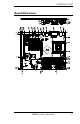
INTRODUCTION Board Dimensions MB820 User’s Manual 3
INSTALLATIONS Installations This section provides information on how to use the jumpers and connectors on the MB820 in order to set up a workable system.
INSTALLATIONS ATX Power Installation The system power is provided to the motherboard with the ATXP1 and ATXP2 ATX power connectors. ATXP2 is a 4-pin 12V power connector. ATXP1 is to be connected to a standard ATX power connector. Installing the Memory The MB820 motherboard supports four DDR memory sockets for a maximum total memory of 4GB in DDR memory type. You can install unbuffered & ECC DDR DIMMs. It supports DDR266 when installed with CPUs that have clock speeds of 400MHz.
INSTALLATIONS Setting the Jumpers Jumpers are used on MB820 to select various settings and features according to your needs and applications. Contact your supplier if you have doubts about the best configuration for your needs. The following lists the connectors on MB820 and their respective functions. Jumper Locations on MB820.............................................................7 JP1: RS232/422/485 (COM2) Selection ..........................................8 JP2: COM1 RS232 +5V/+12V Power Setting.
INSTALLATIONS Jumper Locations on MB820 Jumper Locations on MB820 .............................................................. Page JP1: RS232/422/485 (COM2) Selection..................................................8 JP2: COM1 RS232 +5V/+12V Power Setting ........................................8 JP3: COM2 RS232 +5V/+12V Power Setting ........................................8 JP4: Clear CMOS Contents .......................................................................
INSTALLATIONS JP1: RS232/422/485 (COM2) Selection COM1 is fixed for RS-232 use only. J3, COM2 is selectable for RS232, RS-422 and RS-485. The following table describes the jumper settings for COM2 selection.
INSTALLATIONS JP4: Clear CMOS Contents Use JP4, a 3-pin header, to clear the CMOS contents. Note that the ATX-power connector should be disconnected from the motherboard before clearing CMOS.
INSTALLATIONS JP7: DiskOnChip Address Select JP7 Address D0000-D7FFF D8000-DFFFF (default) JP8: Onboard VGA Enable/Disable Use JP8 to enable or disable the onboard VGA controller.
INSTALLATIONS [ Connectors on MB820 The connectors on MB820 allows you to connect external devices such as keyboard, floppy disk drives, hard disk drives, printers, etc. The following table lists the connectors on MB820 and their respective functions. Connector Locations on MB820 ..........................................12 ATXP1: ATX Power Supply Connector...............................13 ATXP2: ATX 12V Power Connector...................................13 DIMM1, DIMM2: DDR Channel A Connectors............
INSTALLATIONS Connector Locations on MB820 12 MB820 User’s Manual
INSTALLATIONS ATXP1: ATX Power Supply Connector ATXP1 is a 20-pin ATX power supply connector. Refer to the following table for the pin out assignments. 11 1 20 10 Signal Name 3.3V -12V Ground PS-ON Ground Ground Ground -5V +5V +5V Pin # 11 12 13 14 15 16 17 18 19 20 Pin # 1 2 3 4 5 6 7 8 9 10 Signal Name 3.3V 3.
INSTALLATIONS CN1: PS/2 Keyboard and PS/2 Mouse Connectors PS/2 Mouse PS/2 Keyboard Keyboard Mouse Signal Name 1 2 3 4 5 6 1 2 3 4 5 6 Mouse data N.C. GND 5V Mouse clock N.C. Signal Name Keyboard data N.C. GND 5V Keyboard clock N.C. CN2: 4-port USB Connector CN2 is a USB connector consisting of four ports stacked vertically. CN2 Pin 1 2 3 4 Signal Name Ground USB+ USBVcc CN3, J3: Serial Ports CN3 (COM1) is a DB-9 connector, while J3 is a COM2 pin-header connector.
INSTALLATIONS CN4: Parallel Port Connector CN4 is a DB-25 external connector situated on top of the VGA and serial ports. The following table describes the pin-out assignments of this connector.
INSTALLATIONS CN7: USB and LAN RJ45 Connectors CN7 consists of an RJ-45 connector (top) and two stacked USB ports. Refer to the section below for their respective pin assignments. USB0 USB1 Pin # 1 2 3 4 Signal Name Vcc USBUSB+ Ground CN8: Audio Connector CN8 is a 3-jack audio connector beside the USB/RJ45 combo connector. J1: IrDA Connector J1 is used for an optional IrDA connector for wireless communication.
INSTALLATIONS J5, J6: Serial ATA (SATA) Connectors The SATA connectors support serial ATA 150. Each connector can only use one serial ATA hard disk. J6 is port 1 and J5 is port 2. J8, J10: COM3 and COM4 Serial Ports Connector J8 and J10 are both 10-pin headers, as the COM3 and COM4 serial port pin headers supporting RS232. Pin # Signal Name 1 2 3 4 5 6 7 8 9 10 DCD RX TX DTR GND DSR RTS CTS RI NC J9: Wake On LAN Connector J9 is a 3-pin header for the Wake On LAN function on the motherboard.
INSTALLATIONS J11: Digital I/O Connector (4 in, 4 out) This 12-pin Digital I/O connector supports TTL levels and is used to control external devices requiring ON/OFF circuitry. Signal Name IN0 IN1 IN2 IN3 GROUND OUT2 Pin # 1 2 3 4 5 6 Pin # 7 8 9 10 11 12 Signal Name +5V OUT0 Ground OUT1 +12V OUT3 J12: System Function Connector J12 provides connectors for system indicators that provide light indication of the computer activities and switches to change the computer status.
INSTALLATIONS Power LED: Pins 11 - 15 The power LED indicates the status of the main power switch. Pin # 11 12 13 14 15 Signal Name Power LED No connect Ground No connect Ground SMI/Hardware Switch: Pins 6 and 16 This connector supports the "Green Switch" on the control panel, which, when pressed, will force the system into the power-saving mode immediately.
INSTALLATIONS Hard Disk Drive LED Connector: Pins 10 and 20 This connector connects to the hard drive activity LED on control panel. This LED will flash when the HDD is being accessed.
INSTALLATIONS FDD1: Floppy Drive Connector FDD1 Signal Name Ground Ground Ground Ground Ground Ground Ground Ground Ground Ground Ground Ground Ground Ground Ground Ground Ground Pin # 1 3 5 7 9 11 13 15 17 19 21 23 25 27 29 31 33 Pin # 2 4 6 8 10 12 14 16 18 20 22 24 26 28 30 32 34 MB820 User’s Manual Signal Name RM/LC No connect No connect Index Motor enable 0 Drive select 1 Drive select 0 Motor enable 1 Direction Step Write data Write gate Track 00 Write protect Read data Side 1 select Diskette ch
INSTALLATIONS IDE, IDE2: Primary and Secondary IDE Connectors IDE1 IDE2 22 Signal Name Reset IDE Host data 7 Host data 6 Host data 5 Host data 4 Host data 3 Host data 2 Host data 1 Host data 0 Ground DRQ0 Host IOW Host IOR IOCHRDY DACK0 IRQ14 Address 1 Address 0 Chip select 0 Activity Pin # 1 3 5 7 9 11 13 15 17 19 21 23 25 27 29 31 33 35 37 39 Pin # 2 4 6 8 10 12 14 16 18 20 22 24 26 28 30 32 34 36 38 40 Signal Name Ground Host data 8 Host data 9 Host data 10 Host data 11 Host data 12 Host data 13
INSTALLATIONS Watchdog Timer Configuration The WDT is used to generate a variety of output signals after a user programmable count. The WDT is suitable for use in the prevention of system lock-up, such as when software becomes trapped in a deadlock. Under these sort of circumstances, the timer will count to zero and the selected outputs will be driven. Under normal circumstance, the user will restart the WDT at regular intervals before the timer counts to zero.
INSTALLATIONS mov cl, 0F5h call Read_Reg and al, NOT 08h call Write_Reg ;set count mode as second pop ax mov cl, 0F6h call Write_Reg ;set watchdog timer mov al, 01h mov cl, 30h call Write_Reg ;watchdog enabled call Lock_Chip ret Enable_And_Set_Watchdog Endp ;[]=============================================== ; Name : Disable_Watchdog ; IN : None ; OUT : None ;[]=============================================== Disable_Watchdog Proc Near call Unlock_Chip mov cl, 07h mov al, 08h call Write_Reg ;switch to
INSTALLATIONS ; Name : Unlock_Chip ; IN : None ; OUT : None ;[]=============================================== Unlock_Chip Proc Near mov dx, 2Eh mov al, 87h out dx, al out dx, al ret Unlock_Chip Endp ;[]================================================ ; Name : Lock_Chip ; IN : None ; OUT : None ;[]================================================ Unlock_Chip Proc Near mov dx, 2Eh mov al, 0AAh out dx, al ret Unlock_Chip Endp ;[]================================================ ; Name : Write_Reg ; IN : CL - r
INSTALLATIONS ; Name : Read_Reg ; IN : CL - register index ; OUT : AL - Value to read ;[]================================================ === Read_Reg Proc Near mov al, cl mov dx, 2Eh out dx, al inc dx in al, dx ret Read_Reg Endp ;[]================================================ 26 MB820 User’s Manual
BIOS SETUP BIOS Setup This chapter describes the different settings available in the Award BIOS that comes with the motherboard. The topics covered in this chapter are as follows: BIOS Introduction .........................................................................28 BIOS Setup .....................................................................................28 Standard CMOS Setup .................................................................30 Advanced BIOS Features ..........................
BIOS SETUP BIOS Introduction The Award BIOS (Basic Input/Output System) installed in your computer system’s ROM supports Intel® Pentium® 4 processors. The BIOS provides critical low-level support for a standard device such as disk drives, serial ports and parallel ports. It also adds virus and password protection as well as special support for detailed fine-tuning of the chipset controlling the entire system.
BIOS SETUP Phoenix - AwardBIOS CMOS Setup Utility Standard CMOS Features Advanced BIOS Features Advanced Chipset Features Integrated Peripherals Power Management Setup PnP/PCI Configurations PC Health Status Frequency/Voltage Control Load Fail-Safe Defaults Load Optimized Defaults Set Supervisor Password Set User Password Save & Exit Setup Exit Without Saving ESC : Quit F10 : Save & Exit Setup á â à ß : Select Item Time, Date, Hard Disk Type… The section below the setup items of the Main Menu display
BIOS SETUP Standard CMOS Setup “Standard CMOS Setup” choice allows you to record some basic hardware configurations in your computer system and set the system clock and error handling. If the motherboard is already installed in a working system, you will not need to select this option. You will need to run the Standard CMOS option, however, if you change your system hardware configurations, the onboard battery fails, or the configuration stored in the CMOS memory was lost or damaged.
BIOS SETUP Time The time format is: Hour : 00 to 23 Minute : 00 to 59 Second : 00 to 59 To set the time, highlight the “Time” field and use the / or +/- keys to set the current time. IDE Primary HDDs / IDE Secondary HDDs The onboard PCI IDE connectors provide Primary and Secondary channels for connecting up to four IDE hard disks or other IDE devices. Each channel can support up to two hard disks; the first is the “Master” and the second is the “Slave”.
BIOS SETUP Video This field selects the type of video display card installed in your system. You can choose the following video display cards: EGA/VGA For EGA, VGA, SEGA, SVGA or PGA monitor adapters. (default) CGA 40 Power up in 40 column mode. CGA 80 Power up in 80 column mode. MONO For Hercules or MDA adapters. Halt On This field determines whether or not the system will halt if an error is detected during power up. No errors The system boot will not be halted for any error that may be detected.
BIOS SETUP Advanced BIOS Features This section allows you to configure and improve your system and allows you to set up some system features according to your preference.
BIOS SETUP First/Second/Third Boot Device These fields determine the drive that the system searches first for an operating system. The options available include Floppy, LS120, Hard Disk, CDROM, ZIP100, USB-FDD, USB-CDROM and Disable. Boot Other Device These fields allow the system to search for an operating system from other devices other than the ones selected in the First/Second/Third Boot Device. Swap Floppy Drive This item allows you to determine whether or not to enable Swap Floppy Drive.
BIOS SETUP Security Option This field allows you to limit access to the System and Setup. The default value is Setup. When you select System, the system prompts for the User Password every time you boot up. When you select Setup, the system always boots up and prompts for the Supervisor Password only when the Setup utility is called up. APIC Mode APIC stands for Advanced Programmable Interrupt Controller. The default setting is Enabled.
BIOS SETUP Advanced Chipset Features This Setup menu controls the configuration of the chipset. Phoenix - AwardBIOS CMOS Setup Utility Advanced Chipset Features DRAM Timing Selectable CAS Latency Time Active to Precharge Delay DRAM RAS# to CAS# Delay DRAM RAS# Precharge Memory Frequency For System BIOS Cacheable Video BIOS Cacheable Memory Hole at 15M-16M Delay Prior to Thermal AGP Aperture Size (MB) Init Display First DRAM Data Integrity Mode By SPD 2.
BIOS SETUP Memory Frequency For This field sets the frequency of the DRAM memory installed. The default setting is Auto. The other settings are DDR266, DDR333, DDR320 and DDR400. System BIOS Cacheable The setting of Enabled allows caching of the system BIOS ROM at F000h-FFFFFh, resulting in better system performance. However, if any program writes to this memory area, a system error may result.
BIOS SETUP Integrated Peripherals This section sets configurations for your hard disk and other integrated peripherals. The first screen shows three main items for user to select. Once an item selected, a submenu appears. Details follow.
BIOS SETUP Phoenix - AwardBIOS CMOS Setup Utility SuperIO Device Onboard FDC Controller Onboard Serial Port 1 Onboard Serial Port 2 UART Mode Select RxD , TxD Active IR Transmission Delay UR2 Duplex Mode Use IR Pins Onboard Parallel Port Parallel Port Mode EPP Mode Select ECP Mode Use DMA Onboard Serial Port 3 Serial Port 3 Use IRQ Onboard Serial Port 4 Serial Port 4 Use IRQ Chip Select Pin Enabled 3F8/IRQ4 2F8/IRQ3 Normal Hi, Lo Enabled Half IR-Rx2Tx2 378/IRQ7 SPP EPP1.
BIOS SETUP On-Chip Serial ATA The default setting of Auto allows the Serial ATA drive to be enabled, when the system detects one. USB Controller The options for this field are Enabled and Disabled. By default, this field is set to Enabled. USB 2.0 Controller The options for this field are Enabled and Disabled. By default, this field is set to Disabled. In order to use USB 2.0, necessary OS drivers must be installed first. USB Keyboard Support The options for this field are Enabled and Disabled.
BIOS SETUP UART Mode Select This field determines the UART 2 mode in your computer. The default value is Normal. Other options include IrDA and ASKIR. Parallel Port Mode This field allows you to determine parallel port mode function. SPP Standard Printer Port EPP Enhanced Parallel Port ECP Extended Capabilities Port Chip Select Pin This item is used in conjunction with the digital I/O function.
BIOS SETUP Power Management Setup The Power Management Setup allows you to save energy of your system effectively.
BIOS SETUP Video Off Method This field defines the Video Off features. There are three options. V/H SYNC + Blank Default setting, blank the screen and turn off vertical and horizontal scanning. DPMS Allows BIOS to control the video display. Blank Screen Writes blanks to the video buffer. Video Off In Suspend When enabled, the video is off in suspend mode. The default setting is Yes. Suspend Type The default setting for the Suspend Type field is Stop Grant.
BIOS SETUP Power On by Ring This field enables or disables the power on of the system through the modem connected to the serial port or LAN. Wake Up On LAN Enable this field to allow wake up function through the onboard LAN. Resume by Alarm This field enables or disables the resumption of the system operation. When enabled, the user is allowed to set the Date and Time.
BIOS SETUP PNP/PCI Configurations This option configures the PCI bus system. All PCI bus systems on the system use INT#, thus all installed PCI cards must be set to this value.
BIOS SETUP PC Health Status This section shows the parameters in determining the PC Health Status. These parameters include temperatures, fan speeds and voltages. Phoenix - AwardBIOS CMOS Setup Utility PC Health Status CPU Warning Temperature System Temp. CPU Temp CPU FAN Speed (FAN1) System FAN Speed (FAN3) Chassis FAN Speed (FAN2) Disabled ITEM HELP Menu Level Vcore (V) +3.3V +5V +12V -12V VBAT 5VSB(V) Shutdown Temperature CPU Fan Failure Warning Disabled Disabled Sys.
BIOS SETUP Frequency/Voltage Control This section shows the user how to configure the processor frequency. Phoenix - AwardBIOS CMOS Setup Utility Frequency/Voltage Control Auto Detect DIMM/PCI Clk Disabled Spread Spectrum Disabled ITEM HELP Menu Level Auto Detect DIMM/PCI Clk This field enables or disables the auto detection of the PCI clock. Spread Spectrum This field sets the value of the spread spectrum. The default setting is Disabled. This field is for CE testing use only.
BIOS SETUP Load Fail-Safe Defaults This option allows you to load the troubleshooting default values permanently stored in the BIOS ROM. These default settings are non-optimal and disable all high-performance features. Load Setup Defaults This option allows you to load the default values to your system configuration. These default settings are optimal and enable all high performance features. Set Supervisor/User Password These two options set the system password.
DRIVERS INSTALLATION Drivers Installation This section describes the installation procedures for software and drivers under the Windows 98SE, Windows ME, Windows 2000 and Windows XP. The software and drivers are included with the motherboard. If you find the items missing, please contact the vendor where you made the purchase.
DRIVERS INSTALLATION Intel 875P Chipset Software Intallation Utility The Intel® 875P Chipset Drivers should be installed first before the software drivers to enable Plug & Play INF support for Intel® chipset components. Follow the instructions below to complete the installation under Windows 98SE/ME/2000/XP. 1. Insert the CD that comes with the motherboard and the screen below would appear. Click Intel Chipsets and then Intel(R) 875P Chipset Drivers. 2. Click Intel(R) Chipset Software Intallation Utility.
DRIVERS INSTALLATION 3. When the Welcome screen appears, click Next to continue. 4. Click Yes to accept the software license agreement and proceed with the installation process.
DRIVERS INSTALLATION 5. On Readme Information screen, click Next to continue the installation. 6. The Setup process is now complete. Click Finish to restart the computer and for changes to take effect. When the computer has restarted, the system will be able to find some devices. Restart your computer when prompted.
DRIVERS INSTALLATION Realtek AC97 Codec Audio Driver Installation Follow the steps below to install the Realtek AC97 Codec Audio Drivers. 1. Insert the CD that comes with the motherboard and the screen below would appear. Click Intel(R) Chipsets, then Intel(R) 875P Chipset Family Drivers. Click Realtek AC97 Codec Audio Drivers to start installation. 2. Click Finish to restart the computer and for changes to take effect. .
DRIVERS INSTALLATION Intel PRO LAN Drivers Installation The Intel® PRO LAN drivers support both Intel® PRO/100 and PRO/1000 drivers. Follow the steps below to complete the installation. 1. Insert the CD that comes with the motherboard and the screen below would appear. Click on LAN Card on the left side to make the LAN drivers selection. Click on Intel(R) PRO LAN Drivers. 2. Click Install Software to continue. 3. When prompted, click Restart to restart the computer for new settings to take effect.
DRIVERS INSTALLATION VGA Drivers Installation To install the SMI VGA drivers (SMI SM712), follow the steps below to proceed with the installation. 1. Insert the CD that comes with the MB820 and the screen below would appear. Click VGA Card on the left side. 2. On the right side of the screen, click on SMI712 VGA Driver.
DRIVERS INSTALLATION 3. A Welcome screen would then appear. Click Next to start copying of files needed for the driver installation. 4. After file copying is done, restart the computer when prompted for changes to take effect.