MI940 LGA775 Core™ 2 Duo Intel® 945GC Chipset Mini-ITX Motherboard USER’S MANUAL Version 1.
Acknowledgments Award is a registered trademark of Award Software International, Inc. PS/2 is a trademark of International Business Machines Corporation. Intel is a trademark or registered trademark of Intel Corporation. Microsoft Windows is a registered trademark of Microsoft Corporation. Winbond is a registered trademark of Winbond Electronics Corporation. All other product names or trademarks are properties of their respective owners.
Table of Contents Introduction ....................................................... 1 Checklist .............................................................................. 1 Product Description ............................................................. 2 Specifications ...................................................................... 3 Board Dimensions ............................................................... 4 Installations .......................................................
This page is intentionally left blank.
INTRODUCTION Introduction Checklist Your MI940 Core 2 Duo motherboard package should include the items listed below: • The MI940 motherboard • This User’s manual • 1 x I/O shield • 1 x IDE cable • 1 x SATA cable • 1 CD containing the following: • Chipset Drivers • Flash Memory Utility MI940 User’s Manual 1
INSTALLATIONS Product Description The MI940 Mini-ITX motherboard is designed for LGA775 processors such as the Intel® Core™2 Duo, and Pentium D / Pentium 4 processors with up to 800MHz FSB. It is based on the Intel’s 945GC Express chipset and it comes with two DDR2 memory slots and 2GB memory capacity for faster system responsiveness. MI940 comes with the Intel® 945GC integrated graphics and Chrontel CH7307 to support for CRT and DVI display interface.
INTRODUCTION Specifications Form Factor Processor FSB Chipset BIOS Memory VGA DVI LAN USB SATA II IDE Audio LPC I/O Hardware Monitor Edge Connectors On Board Headers / Connectors Expansion Watchdog Timer Digital IO Other Power Connector System Voltage Board Size Mini ITX (for performance desktop market) Socket LGA775, Supports the Intel Core 2 Duo and Intel Pentium D processors.
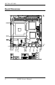
INSTALLATIONS Board Dimensions 4 MI940 User’s Manual
INSTALLATIONS Installations This section provides information on how to use the jumpers and connectors on the MI940 in order to set up a workable system. The topics covered are: Installing the CPU ................................................................................. 6 ATX Power Installation ......................................................................... 6 Installing the Memory ........................................................................... 7 Setting the Jumpers............
INSTALLATIONS Installing the CPU The MI940 motherboard supports an LGA 775 processor socket for Intel® Core 2 Duo processors. The LGA 775 processor socket comes with a lever to secure the processor. Refer to the pictures below, from left to right, on how to place the processor into the CPU socket. Please note that the cover of the LGA775 socket must always be installed during transport to avoid damage to the socket.
INSTALLATIONS Installing the Memory The MI940 motherboard supports four DDR2 memory sockets for a maximum total memory of 2GB in DDR memory type. It supports DDR2 400/533/667MHz. Basically, the system memory interface has the following features: Supports two 64-bit wide DDR data channels Available bandwidth up to 5.3GB/s (DDR2 667) for single channel mode and 10.6GB/s (DDR2 667) for dual channel mode. Supports 256Mb, 512Mb, 1Gb DDR2 technologies.
INSTALLATIONS Setting the Jumpers Jumpers are used on the motherboard are used to select various settings and features according to your needs and applications. Contact your supplier if you have doubts about the best configuration for your needs. The following lists the connectors and their respective functions. Jumper Locations on MI940 .................................................................. 9 JP5: Clear CMOS Contents .................................................................
INSTALLATIONS Jumper Locations on MI940 Jumper Locations on MI940...................................................... Page JP1, JP2, JP3: RS232/422/485 (COM2) Selection ....................... 10 JP5: Clear CMOS Contents ..........................................................
INSTALLATIONS JP1, JP2, JP3: RS232/422/485 (COM2) Selection COM1 is fixed for RS-232 use only. COM2 is selectable for RS232, RS-422 and RS-485. ID394: COM3 and COM4 are fixed for RS-232 use only. The following table describes the jumper settings for COM2 selection.
INSTALLATIONS Connectors on MI940 The connectors on MI940 allow you to connect external devices such as keyboard, floppy disk drives, hard disk drives, printers, etc. The following table lists the connectors on MI940 and their respective functions. Connector Locations on MI940 ....................................................................... 12 ATX2: 24-pin ATX Power Connector ............................................................. 13 ATX1: ATX 12V Power Connector ..............................
INSTALLATIONS Connector Locations on MI940 ATX2: 24-pin ATX Power Connector ................................................................................................... 13 ATX1: ATX 12V Power Connector ....................................................................................................... 13 CPU_FAN1: CPU Fan Power Connector .............................................................................................. 13 SYSFAN1, 2: System Fan Power Connectors.......................
INSTALLATIONS ATX2: 24-pin ATX Power Connector Signal Name 3.3V -12V Ground PS-ON Ground Ground Ground -5V +5V +5V +5V Ground Pin # 13 14 15 16 17 18 19 20 21 22 23 24 Pin # 1 2 3 4 5 6 7 8 9 10 11 12 Signal Name 3.3V 3.3V Ground +5V Ground +5V Ground Power good 5VSB +12V +12V +3.
INSTALLATIONS CN3: PS/2 Keyboard and PS/2 Mouse Connectors Keyboard Signal Pin # Mouse Signal Keyboard data 1 Mouse data N.C. 2 N.C. GND 3 GND 5V 4 5V Mouse (top) Keyboard clock 5 Mouse clock Keyboard (bottom) N.C. 6 N.C. CN1, J1: COM1/2 Serial Ports CN1 (COM1) is a DB-9 connector, while J1 is a COM pin-header connector.
INSTALLATIONS CN4: VGA & DVI-D Connector Signal Name Red Blue GND GND VCC N.C. HSYNC DDCCLK Pin # 1 3 5 7 9 11 13 15 Pin # Signal Name 2 Green 4 N.C. 6 GND 8 GND 10 GND 12 DDCDATA 14 VSYNC Signal Name DATA2GND N.C. DDCDATA DATA1GND N.C. GND Pin # 1 3 5 7 9 11 13 15 DATA0GND N.C. CLK+ 17 19 21 23 Pin # Signal Name 2 DATA2+ 4 N.C. 6 DDCCLK 8 N.C. 10 DATA1+ 12 N.C. 14 VCC 16 Hot Plug Detect 18 DATA0+ 20 N.C. 22 GND 24 CLK- CN2: USB2/3 Connector CN5: Audio Connector CN5 is a 3-jack audio connector.
INSTALLATIONS CN6: Intel 82574L PCI-express Gigabit LAN and USB0/1 Connector CN7, CN8, CN9, CN10: SATA HDD Connectors Pin # Signal Name 1 Ground 2 TX+ 3 TX4 Ground 5 RX6 RX+ 7 Ground IDE1: Primary IDE Connectors Signal Name Pin # Reset IDE 1 Host data 7 3 Host data 6 5 Host data 5 7 Host data 4 9 Host data 3 11 Host data 2 13 Host data 1 15 Host data 0 17 Ground 19 DRQ0 21 Host IOW 23 Host IOR 25 IOCHRDY 27 DACK0 29 IRQ14 31 Address 1 33 IDE1 Address 0 35 Chip select 0 37 Activity 39 16 Pin # 2 4 6 8 10
INSTALLATIONS J3: Digital I/O Connector (4 in, 4 out) This 10-pin digital I/O connector supports TTL levels and is used to control external devices requiring ON/OFF circuitry.
INSTALLATIONS Hard Disk Drive LED Connector: Pins 3 and 4 This connector connects to the hard drive activity LED on control panel. This LED will flash when the HDD is being accessed. Pin # 4 3 Signal Name HDD Active 5V Reset Switch: Pins 5 and 6 The reset switch allows the user to reset the system without turning the main power switch off and then on again. Orientation is not required when making a connection to this header.
INSTALLATIONS ID394 LPC Serial Ports Adapter (option) J1 J2: COM3/4/5/6 Serial Ports J1 - COM3/4 pin-header connector. PIN1~PIN10 COM3 PIN11~PIN20 COM4 J2 - COM5/6 pin-header connector.
INSTALLATIONS This page is intentionally left blank.
BIOS SETUP BIOS Setup This chapter describes the different settings available in the Award BIOS that comes with the board. The topics covered in this chapter are as follows: BIOS Introduction ........................................................................ 21 BIOS Setup ................................................................................... 21 Standard CMOS Setup ................................................................. 23 Advanced BIOS Features .................................
BIOS SETUP BIOS Introduction The Award BIOS (Basic Input/Output System) installed in your computer system’s ROM supports Intel processors. The BIOS provides critical low-level support for a standard device such as disk drives, serial ports and parallel ports. It also adds virus and password protection as well as special support for detailed fine-tuning of the chipset controlling the entire system.
BIOS SETUP Phoenix - AwardBIOS CMOS Setup Utility Standard CMOS Features Advanced BIOS Features Advanced Chipset Features Integrated Peripherals Power Management Setup PnP/PCI Configurations PC Health Status Frequency/Voltage Control Load Fail-Safe Defaults Load Optimized Defaults Set Supervisor Password Set User Password Save & Exit Setup Exit Without Saving ESC : Quit F10 : Save & Exit Setup Ç È Æ Å : Select Item Time, Date, Hard Disk Type… The section below the setup items of the Main Menu displays
BIOS SETUP Standard CMOS Setup “Standard CMOS Setup” choice allows you to record some basic hardware configurations in your computer system and set the system clock and error handling. If the motherboard is already installed in a working system, you will not need to select this option. You will need to run the Standard CMOS option, however, if you change your system hardware configurations, the onboard battery fails, or the configuration stored in the CMOS memory was lost or damaged.
BIOS SETUP To set the date, highlight the “Date” field and use the PageUp/ PageDown or +/- keys to set the current time. Time The time format is: Hour : 00 to 23 Minute : 00 to 59 Second : 00 to 59 To set the time, highlight the “Time” field and use the / or +/- keys to set the current time. IDE Channel Master/Slave The onboard Serial ATA connectors provide Primary and Secondary channels for connecting up to four Serial ATA hard disks .
BIOS SETUP Drive A / Drive B These fields identify the types of floppy disk drive A or drive B that has been installed in the computer. The available specifications are: 360KB 1.2MB 720KB 1.44MB 2.88MB 5.25 in. 5.25 in. 3.5 in. 3.5 in. 3.5 in. Video This field selects the type of video display card installed in your system. You can choose the following video display cards: EGA/VGA For EGA, VGA, SEGA, SVGA or PGA monitor adapters. (default) CGA 40 Power up in 40 column mode.
BIOS SETUP Advanced BIOS Features This section allows you to configure and improve your system and allows you to set up some system features according to your preference.
BIOS SETUP Quick Power On Self Test When enabled, this field speeds up the Power On Self Test (POST) after the system is turned on. If it is set to Enabled, BIOS will skip some items. First/Second/Third Boot Device These fields determine the drive that the system searches first for an operating system. The options available include Floppy, LS120, Hard Disk, CDROM, ZIP100, USB-Floppy, USB-ZIP, USB-CDROM, LAN and Disable.
BIOS SETUP Typematic Delay (Msec) When the typematic rate is enabled, this item allows you to set the time interval for displaying the first and second characters. By default, this item is set to 250msec. Security Option This field allows you to limit access to the System and Setup. The default value is Setup. When you select System, the system prompts for the User Password every time you boot up.
BIOS SETUP Advanced Chipset Features This Setup menu controls the configuration of the chipset.
BIOS SETUP DRAM RAS# Precharge This option sets the number of cycles required for the RAS to accumulate its charge before the SDRAM refreshes. Precharge delay (tRAS) The default setting for the Active to Precharge Delay is Auto. System Memory Frequency This field sets the frequency of the DRAM memory installed. The default setting is Auto. The other settings are DDR533 and DDR667. SLP_S4# Assertion Width The default setting is 4 to 5 Sec.
BIOS SETUP Integrated Peripherals This section sets configurations for your hard disk and other integrated peripherals. The first screen shows three main items for user to select. Once an item selected, a submenu appears. Details follow.
BIOS SETUP Phoenix - AwardBIOS CMOS Setup Utility SuperIO Device POWER ON Function KB Power ON Password Hot Key power ON Onboard FDC Controller Onboard Serial Port 1 Onboard Serial Port 2 UART Mode Select RxD, TxD Active IR Transmission Delay UR2 Duplex Mode Use IR Pins Onboard Parallel Port Parallel Port Mode EPP Mode Select ECP Mode Use DMA PWRON After PWR-Fail BUTTON ONLY Enter Ctrl-F1 Enabled 3F8/IRQ4 2F8/IRQ3 Normal Hi, Lo Enabled Half IR-Rx2Tx2 378/IRQ7 SPP EPP1.
BIOS SETUP On-Chip Serial ATA Setting The fields under the SATA setting includes SATA Mode (IDE), On-Chip Serial ATA (Auto), PATA IDE Mode (Secondary) and SATA Port (P0, P2 is Primary). USB Controller The options for this field are Enabled and Disabled. By default, this field is set to Enabled. USB 2.0 Controller The options for this field are Enabled and Disabled. By default, this field is set to Enabled. In order to use USB 2.0, necessary OS drivers must be installed first.
BIOS SETUP Onboard Serial/Parallel Port These fields allow you to select the onboard serial and parallel ports and their addresses. The default values for these ports are: Serial Port 1 3F8/IRQ4 Serial Port 2 2F8/IRQ3 Parallel Port 378H/IRQ7 UART Mode Select This field determines the UART 2 mode in your computer. The default value is Normal. Other options include IrDA and ASKIR. Parallel Port Mode This field allows you to determine parallel port mode function.
BIOS SETUP Power Management Setup Phoenix - AwardBIOS CMOS Setup Utility Power Management Setup ACPI Function Enabled ACPI Suspend RUN VGABIOS if S3 Resume Power Management Video Off Method Video Off In Suspend Suspend Type Modem Use IRQ Suspend Mode HDD Power Down Soft-Off by PWR-BTTN CPU THRM-Throttling Wake-Up by PCI Card Power On by Ring USB KB Wake-Up From S3 Resume by Alarm Date (of Month) Alarm Time (hh:mm:ss) Alarm S1(POS) Auto User Define DPMS Yes Stop Grant 3 Disabled Disabled Instant-Off 75%
BIOS SETUP Video Off Method This field defines the Video Off features. There are three options. V/H SYNC + Blank Default setting, blank the screen and turn off vertical and horizontal scanning. DPMS Allows BIOS to control the video display. Blank Screen Writes blanks to the video buffer. Video Off In Suspend When enabled, the video is off in suspend mode. Suspend Type The default setting for the Suspend Type field is Stop Grant. Modem Use IRQ This field sets the IRQ used by the Modem.
BIOS SETUP Resume by Alarm This field enables or disables the resumption of the system operation. When enabled, the user is allowed to set the Date and Time. Reload Global Timer Events The HDD, FDD, COM, LPT Ports, and PCI PIRQ are I/O events that can prevent the system from entering a power saving mode or can awaken the system from such a mode. When an I/O device wants to gain the attention of the operating system, it signals this by causing an IRQ to occur.
BIOS SETUP PNP/PCI Configurations This option configures the PCI bus system. All PCI bus systems on the system use INT#, thus all installed PCI cards must be set to this value.
BIOS SETUP PC Health Status This section shows the parameters in determining the PC Health Status. These parameters include temperatures, fan speeds and voltages. Phoenix - AwardBIOS CMOS Setup Utility PC Health Status Shutdown Temperature CPU Warning Temperature North Bridge Temp. CPU Temp. System Temp. System Fan Speed Disabled Disabled 32°C/89°F 39°C/102°F 39°C/102°F 0 RPM CPU Fan Speed Chassis Fan Speed Vcore 12 V 1.8 V 5 V -12V 3.
BIOS SETUP Frequency/Voltage Control Phoenix - AwardBIOS CMOS Setup Utility Frequency/Voltage Control Auto Detect PCI Clk Disabled Spread Spectrum Disabled ITEM HELP Menu Level > Auto Detect PCI Clk This field enables or disables the auto detection of the PCI clock. Spread Spectrum This field sets the value of the spread spectrum. The default setting is Disabled. This field is for CE testing use only.
BIOS SETUP Load Fail-Safe Defaults This option allows you to load the troubleshooting default values permanently stored in the BIOS ROM. These default settings are non-optimal and disable all high-performance features. Load Optimized Defaults This option allows you to load the default values to your system configuration. These default settings are optimal and enable all high performance features. Set Supervisor/User Password These two options set the system password.
DRIVERS INSTALLATION Drivers Installation This section describes the installation procedures for software and drivers under the Windows 2000 and Windows XP. The software and drivers are included with the board. If you find the items missing, please contact the vendor where you made the purchase. The contents of this section include the following: Intel Chipset Software Installation Utility ................................. 44 Intel Graphics Driver Installation ..............................................
DRIVERS INSTALLATION Intel Chipset Software Installation Utility The Intel Chipset Drivers should be installed first before the software drivers to enable Plug & Play INF support for Intel chipset components. Follow the instructions below to complete the installation under Windows 2000/XP. 1. Insert the CD that comes with the board. Click Intel Chipsets and then Intel(R) I945G/GC Chipset Drivers. 2. Click Intel(R) Chipset Software Installation Utility.
DRIVERS INSTALLATION 3. When the Welcome screen appears, click Next to continue. 4. Click Yes to accept the software license agreement and proceed with the installation process.
DRIVERS INSTALLATION 5. On Readme Information screen, click Next to continue the installation. 6. The setup process will be in progress. When Setup completed, click Finish to restart the computer and for changes to take effect.
DRIVERS INSTALLATION VGA Drivers Installation To install the VGA drivers, follow the steps below to proceed with the installation. 1. Insert the CD that comes with the board. Click Intel Chipsets and then Intel(R) I945G/GC Chipset Drivers. Click Intel(R) I945G/GC Chipset Family Graphics Driver.
DRIVERS INSTALLATION 2. When the Welcome screen appears, click Next to continue. 3. Click Yes to to agree with the license agreement and continue the installation. 4. On Readme File Information screen, click Next to continue. 5. On Setup Progress screen, click Next to continue the installation. 6. The Setup process is now complete. Click Finish to restart the computer and for changes to take effect.
DRIVERS INSTALLATION High Definition Codec Audio Driver Installation Follow the steps below to install the Realtek High Definition Codec Audio Drivers. 1. Insert the CD that comes with the motherboard. Click Intel Chipsets and then Intel(R) I945G/GC Chipset Drivers. Click Realtek High Definition Codec Audio Driver.
DRIVERS INSTALLATION 2. When the Welcome screen appears, click Next to continue. 3. Setup has finished installing Realtek High Definition Audio Driver on your computer. Click Finish to restart the computer and for changes to take effect.
DRIVERS INSTALLATION LAN Drivers Installation Follow the steps below to install the Intel 82574L LAN Drivers. 1. Insert the CD that comes with the board. Click LAN Card and then Intel(R) PRO 82574L LAN Drivers. 2. In the next screen, click Install Drivers.
DRIVERS INSTALLATION 3. In the Welcome screen to the InstallShield Wizard for Intel(R) Network Connections, click Next. 4. In the License Agreement screen, click Next to accept the terms in the license agreement. 5. In the Setup Options screen, click the checkbox of Drivers to select it and then click Next. 6. Click Next to begin installation of the drivers. 7. When the InstallShield Wizard is completed, click Finish.
APPENDIX Appendix A. I/O Port Address Map Each peripheral device in the system is assigned a set of I/O port addresses that also becomes the identity of the device. The following table lists the I/O port addresses used.
APPENDIX B. Interrupt Request Lines (IRQ) Peripheral devices use interrupt request lines to notify CPU for the service required. The following table shows the IRQ used by the devices on board.
APPENDIX C. Watchdog Timer Configuration The WDT is used to generate a variety of output signals after a user programmable count. The WDT is suitable for use in the prevention of system lock-up, such as when software becomes trapped in a deadlock. Under these sorts of circumstances, the timer will count to zero and the selected outputs will be driven. Under normal circumstance, the user will restart the WDT at regular intervals before the timer counts to zero.
APPENDIX printf("System will reset after %d seconds\n", bTime); EnableWDT(bTime); return 0; } //======================================================================= void copyright(void) { printf("\n======== Winbond 83627EHF Watch Timer Tester (AUTO DETECT) ========\n"\ " Usage : W627E_WD reset_time\n"\ " Ex : W627E_WD 3 => reset system after 3 second\n"\ " W627E_WD 0 => disable watch dog timer\n"); } //======================================================================= void EnableWDT(int interval) {
APPENDIX //======================================================================= // // THIS CODE AND INFORMATION IS PROVIDED "AS IS" WITHOUT WARRANTY OF ANY // KIND, EITHER EXPRESSED OR IMPLIED, INCLUDING BUT NOT LIMITED TO THE // IMPLIED WARRANTIES OF MERCHANTABILITY AND/OR FITNESS FOR A PARTICULAR // PURPOSE. // //======================================================================= ==== #include "W627EHF.H" #include
APPENDIX Lock_W627EHF(); } //======================================================================= void Set_W627EHF_Reg( unsigned char REG, unsigned char DATA) { Unlock_W627EHF(); outportb(W627EHF_INDEX_PORT, REG); outportb(W627EHF_DATA_PORT, DATA); Lock_W627EHF(); } //======================================================================= unsigned char Get_W627EHF_Reg(unsigned char REG) { unsigned char Result; Unlock_W627EHF(); outportb(W627EHF_INDEX_PORT, REG); Result = inportb(W627EHF_DATA_PORT); Lock
APPENDIX This page is intentionally left blank.
APPENDIX File of the Main.cpp //===================================================================== // THIS CODE AND INFORMATION IS PROVIDED "AS IS" WITHOUT WARRANTY OF ANY // KIND, EITHER EXPRESSED OR IMPLIED, INCLUDING BUT NOT LIMITED TO THE // IMPLIED WARRANTIES OF MERCHANTABILITY AND/OR FITNESS FOR A PARTICULAR // PURPOSE. //===================================================================== #include #include #include #include #include "W627HF.