
Datasheet


Datasheet 99
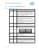
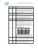
Package Mechanical Specifications and Pin Information
STPCLK# Input
STPCLK# (Stop Clock), when asserted, causes the processor to
enter a low power Stop-Grant state. The processor issues a Stop-
Grant Acknowledge transaction, and stops providing internal clock
signals to all processor core units except the FSB and APIC units.
The processor continues to snoop bus transactions and service
interrupts while in Stop-Grant state. When STPCLK# is deasserted,
the processor restarts its internal clock to all units and resumes
execution. The assertion of STPCLK# has no effect on the bus
clock; STPCLK# is an asynchronous input.
TCK Input
TCK (Test Clock) provides the clock input for the processor Test Bus
(also known as the Test Access Port).
TDI Input
TDI (Test Data In) transfers serial test data into the processor. TDI
provides the serial input needed for JTAG specification support.
TDO Output
TDO (Test Data Out) transfers serial test data out of the processor.
TDO provides the serial output needed for JTAG specification
support.
TEST1,
TEST2,
TEST3,
TEST4,
TEST5,
TEST6
TEST7
Input
Refer to the appropriate platform design guide for further TEST1,
TEST2, TEST3, TEST4, TEST5, TEST6 and TEST7 termination
requirements and implementation details.
THRMDA Other Thermal Diode Anode.
THRMDC Other Thermal Diode Cathode.
THERMTRIP# Output
The processor protects itself from catastrophic overheating by use
of an internal thermal sensor. This sensor is set well above the
normal operating temperature to ensure that there are no false
trips. The processor will stop all execution when the junction
temperature exceeds approximately 125 °C. This is signalled to the
system by the THERMTRIP# (Thermal Trip) pin.
TMS Input
TMS (Test Mode Select) is a JTAG specification support signal used
by debug tools.
TRDY# Input
TRDY# (Target Ready) is asserted by the target to indicate that it is
ready to receive a write or implicit writeback data transfer. TRDY#
must connect the appropriate pins of both FSB agents.
TRST# Input
TRST# (Test Reset) resets the Test Access Port (TAP) logic. TRST#
must be driven low during power on Reset.
VCC Input Processor core power supply.
VSS Input Processor core ground node.
VCCA Input VCCA provides isolated power for the internal processor core PLLs
.
VCCP Input Processor I/O Power Supply.
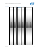
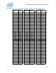
Table 19. Signal Description (Sheet 7 of 8)
Name Type Description