
Hub Datasheet


Intel
®
E7505 Chipset MCH Datasheet 103
Register Description
3.7.8 MLT1—Master Latency Timer (Scratch Pad) Register
(D1:F0)
Address Offset: 0Dh
Default Value: 00h
Attribute: R/W, RO
Size: 8 bits
This functionality is not applicable. It is described here since these bits should be implemented as a
read/write to prevent standard PCI-to-PCI bridge configuration software from getting “confused.”
3.7.9 HDR1—Header Type Register (D1:F0)
Address Offset: 0Eh
Default Value: 01h
Attribute: RO
Size: 8 bits
This register identifies the header layout of the configuration space. No physical register exists at
this location.
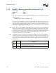
Bits
Default,
Access
Description
7:3
00000b
R/W
Scratch pad MLT (NA7.3). These bits return the value with which they are written;
however, they have no internal function and are implemented as a scratch pad merely to
avoid confusing software.
2:0 Reserved
Bits
Default,
Access
Description
7:0
01h
RO
Header Type Register (HDR). This read only field always returns 01h to indicate that
MCH device 1 is a single function device with bridge header layout.