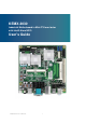
KEMX-2030 Industrial Motherboard in Mini-ITX form factor with Intel® Atom N270 User’s Guide KEMX-2030 User’s Manual I
Contact Info: Quanmax Inc. 4F, No. 415, Ti-Ding Blvd. Sec. 2NeiHu District, Taipei 114Taiwan Tel: +886-2-2799-2789 Fax: +886-2-2799-7399 Visit our site at: www.quanmax.com © 2008 Quanmax Inc. All rights reserved. The information in this user’s guide is provided for reference only. Quanmax does not assume any liability arising out of the application or use of the information or products described herein.
Content Content Content....................................................................................................................... 3 Figures ....................................................................................................................... 5 Tables ......................................................................................................................... 6 Safety Instructions .....................................................................................
Content Security Menu ........................................................................................ 49 Exit Menu ............................................................................................... 50 Chapter 5 Driver Installation .................................................................................. 52 Appendix A System Resources .............................................................................. 53 Appendix B DIO (Digital I/O) KIT User Guide ...................
Figures Figures Figure 1 Block Diagram ............................................................................. 18 Figure 2 Mechanical Dimensions ............................................................... 19 Figure 3 Jumper Connector ....................................................................... 20 Figure 4 Jumper and Connector Locations ................................................ 21 Figure 5 Rear Panel IO .............................................................................
Tables Tables Table 1 KEMX-2030 Specification .............................................................. 17 Table 2 Jumper List .................................................................................... 22 Table 3 JP1 Backlight Enable Selection .................................................. 22 Table 4 JP2 Backlight & Panel Power Selection ...................................... 22 Table 5 JP3 Clear CMOS Selection .........................................................
Tables Table 35 MPCI1, Mini-PCI Socket .............................................................. 33 Table 36 PCI1, PCI slots ............................................................................ 35 Table 37 ATX1, +12V Power Input Connector ............................................ 36 Table 38 Parallel Port Wafer ...................................................................... 36 Table 39 BIOS Main Menu .........................................................................
Safety Instructions Safety Instructions Before You Begin Before handling the product, read the instructions and safety guidelines on the following pages to prevent damage to the product and to ensure your own personal safety. Refer to the “Advisories” section in the Preface for advisory conventions used in this user’s guide, including the distinction between Warnings, Cautions, Important Notes, and Notes. Always use caution when handling/operating a computer.
Safety Instructions 3. 4. Follow the guidelines provided in “Preventing Electrostatic Discharge” on the following page. Disconnect any telephone or telecommunications lines from the computer. In addition, take note of these safety guidelines when appropriate: To help avoid possible damage to system boards, wait five seconds after turning off the computer before removing a component, removing a system board, or disconnecting a peripheral device from the computer.
Safety Instructions or packaging. Handle all sensitive components at an ESD workstation. If possible, use antistatic floor pads and workbench pads. Handle components and boards with care. Don’t touch the components or contacts on a board. Hold a board by its edges or by its metal mounting bracket. Do not handle or store system boards near strong electrostatic, electromagnetic, magnetic, or radioactive fields.
Preface Preface How to Use This Guide This guide is designed to be used as step-by-step instructions for installation, and as a reference for operation, troubleshooting, and upgrades. NOTE Driver downloads and additional information are available under Downloads on our web site: www.quanmax.com. Unpacking When unpacking, follow these steps: 1. After opening the box, save it and the packing material for possible future shipment. 2. Remove all items from the box.
Preface area (domestic environment) is likely to cause harmful interference, in which case the user will be required to correct the interference (take adequate measures) at their own expense. Changes or modifications not expressly approved by Quanmax could void the user's authority to operate the equipment.
Preface date of purchase. To reduce risk of damage, returns of product must be in a Quanmax shipping container. If the original container has been lost or damaged, new shipping containers may be obtained from Quanmax Customer Service at a nominal cost. Quanmax owns all parts removed from repaired products. Quanmax uses new and reconditioned parts made by various manufacturers in performing warranty repairs and building replacement products.
Preface properties as electrical resistance and thermal conductivity. Extreme moisture buildup inside the system can result in electrical shorts, which can cause serious damage to the system. Buildings in which climate is controlled usually maintain an acceptable level of humidity for system equipment. However, if a system is located in an unusually humid location, a dehumidifier can be used to maintain the humidity within an acceptable range.
Preface Uninterruptible power supply (UPS) systems offer the most complete protection against variations on power because they use battery power to keep the server running when AC power is lost. The battery is charged by the AC power while it is available, so when AC power is lost, the battery can provide power to the system for a limited amount of time, depending on the UPS system.
Chapter 1 Chapter 1 Introduction Overview The KEMX-2030 is a Mini-ITX form factor industrial motherboard combining the latest Intel 45nm Intel® Atom™ processor with the high integration of the Intel® 945GSE/ ICH7-M chipset. The new architecture of Atom™ N270 enable the lowest power consumption and smallest form factor for thin client and fundamental use.
Chapter 1 Product Specifications KEMX-2030` CPU Support Intel® Atom™ N270 Chipset Intel® 945GSE + ICH7-M Memory 1x DDR2 400/533 SO-DIMM Socket, up to 2GB BIOS AMI PnP 8Mb SPI ROM Display Integrated on Intel® 945GSE Chipset 18/24-bit dual-channel LVDS from Chrontel CH7308 18-bit Dual channel LVDS from 945GSE optional 1x VGA LAN 1x RJ-45, Fast Ethernet (Realtek RTL8102E) or 1x RJ-45, Gigabit Ethernet (Realtek RTL8111C optional) Audio HD Audio Codec, supports Line-in, Line-out & Microphone (Rea
Chapter 1 System Block Diagram Figure 1 Block Diagram KEMX-2030 User’s Manual 18
Chapter 1 Mechanical Dimensions Figure 2 Mechanical Dimensions KEMX-2030 User’s Manual 19
Chapter 2 Chapter 2 Hardware Settings Overview This chapter provides the definitions and locations of jumpers, headers, and connectors. Jumpers The product has several jumpers which must be properly configured to ensure correct operation. Figure 3 Jumper Connector For a three-pin jumper (see Figure 3), the jumper setting is designated “1-2” when the jumper connects pins 1 and 2. The jumper setting is designated “2-3” when pins 2 and 3 are connected and so on.
Chapter 2 Jumper Settings and Pin Definitions For jumper and connector locations, please refer to the diagrams below.
Chapter 2 Jumper Settings To ensure correct system configuration, the following section describes how to set the jumpers to enable/disable or change functions. For jumper descriptions, please refer to the table below.
Chapter 2 Table 6 JP4 Jumper COM1 Signal / Power Selection Setting 1-3 Short 3-5 Short 5-7 Short 1 Function Pin 1 of COM1 = +12V Pin 1 of COM1 = +5V Pin 1 of COM1 = +5V Pin 1 of COM1 = DCD@RS232, TX-@RS422, DATA-@RS485 (Default) Pin 9 of COM1 = +12V Pin 9 of COM1 = +5V Pin 9 of COM1 = +5V Pin 9 of COM1 = RI (Default) 7-9 Short 2 2-4 Short 4-6 Short 6-8 Short 8-10 Short Pitch:2.
Chapter 2 Rear Panel Pin Assignments Figure 5 Rear Panel IO Table 10 Rear Panel Connector List Label Function AUDIO1 3-Port Audio phone jack USB2 USB2.0 Port 2 , 3 Type A Connector CN9 USB2.
Chapter 2 Table 13 CN9, USB2.
Chapter 2 Table 15 CN 10, PS/2 KB/MS Connector Pin Signal Function 1 KBDAT Keyboard Data 2 NC No Connect 3 GND Ground 4 KB5V +5VSB Power Source 5 KBCLK Keyboard Clock 6 NC No Connect 7 MSDAT Mouse Data 8 NC No Connect 9 GND Ground 10 KB5V +5VSB Power Source 11 MSCLK Mouse Clock 12 NC No Connect MINI DIN DIP 6/6P MH11061-P36-4F 90D(F) Kb/Ms for PC99 CONNECTOR [FOXCONN] Table 16 J1, +12V Power Input Connector Pin Signal 1 NC 2 +12V 3 GND DC POWER DIP 3PIN φ 2.
Chapter 2 Main Board Pin Assignments Table 17 Internal Connector List Label CN2 CN3 CN4 CN5 CN6 CN7 CN8 CN11 DIMM1 FP1 FP2 LVDS1 IDE1 SATA1 SATA2 USB3 USB4 COM2 COM3 COM4 PCIE1 MPCI1 PCI1 ATX1 LPT1 Function Panel Backlight Wafer Digital Input / Output Pin Header Front Panel Audio Pin Header CD-In Connector Pin Header SPDIF Pin Header Audio AMP Right Output Wafer Audio AMP Left Output Wafer AT Power Wafer DDR2 Memory SO-DIMM Socket Front Panel 1 Pin Header Front Panel 2 Pin Header LVDS Panel Pin Header 44P
Chapter 2 Table 19 CN3, Digital Input / Output Pin Header Pin Signal Pin Signal 1 Digital Output 0 2 Digital Input 0 3 Digital Output 1 4 Digital Input 1 5 Digital Output 2 6 Digital Input 2 7 Digital Output 3 8 Digital Input 3 9 +5V 10 GND Pitch:2.54mm [YIMTEX 3322*05SAGR(6T] Table 20 CN4, Front Panel Audio Pin Header Pin Signal Pin Signal 1 MIC2-L 2 Audio GND 3 MIC2-R 4 ACZ_DET# 5 Line2-R 6 MIC2_JD 7 FIO_Sense 8 Key 9 Line2-L 10 Line2_JD Pitch:2.
Chapter 2 Table 23 CN7, Audio AMP Right Output Wafer Pin Signal Name 1 Speaker+ 2 Speaker- Pitch=2.0mm WAFER [YIMTEX 503PW1*02STR] Table 24 CN8, Audio AMP Left Output Wafer Pin Signal Name 1 Speaker+ 2 Speaker- Pitch=2.0mm WAFER [YIMTEX 503PW1*02STR] Table 25 CN11, AT Power Output Wafer Pin Signal Name 1 +12V 2 GND 3 GND 4 +5V Pitch: 5.
Chapter 2 Table 27 FP2, Front Panel 2 Pin Header Pin Signal Pin Signal 1 Power LED + 2 Power Button + 3 NC 4 Power Button - 5 Power LED - 6 NC 7 Keyboard Lock 8 SMBus Data 9 GND 10 SMBus Clock Pitch:2.
Chapter 2 Table 29 IDE1, Primary 44-pin IDE Box Header Signal Name Pin Pin Signal Name Reset IDE 1 2 GND IDE Data 7 3 4 IDE Data 8 IDE Data 6 5 6 IDE Data 9 IDE Data 5 7 8 IDE Data 10 IDE Data 4 9 10 IDE Data 11 IDE Data 3 11 12 IDE Data 12 IDE Data 2 13 14 IDE Data 13 IDE Data 1 15 16 IDE Data 14 IDE Data 0 17 18 IDE Data 15 Ground 19 20 NC DREQ0 21 22 GND IDEIOW# 23 24 GND IDEIOR# 25 26 GND IDEIORDY 27 28 CBSEL DACK0# 29 30 GND IDEIRQ14 31
Chapter 2 Table 31 USB3, USB2.0 Port 4, 5 Pin Header Pin Signal Name Pin Signal Name 1 +5V 2 +5V 3 USB4- 4 USB5- 5 USB4+ 6 USB5+ 7 GND 8 GND 9 KEY 10 GND Pitch:2.54mm [YIMTEX 3322*05SAGR(6T) -09] Table 32 USB4, USB2.0 Port 6, 7 Pin Header Pin Signal Name Pin Signal Name 1 +5V 2 +5V 3 USB6- 4 USB7- 5 USB6+ 6 USB7+ 7 GND 8 GND 9 KEY 10 GND Pitch:2.
Chapter 2 Table 34 PCIE1 PCIE slots PCIE slots Pin Side B Side A 1 12V 3.3V 2 12V 3.3V 3 3.
Chapter 2 33 35 37 39 41 43 45 47 49 51 53 55 57 59 61 63 65 67 69 71 73 75 77 79 81 83 85 87 89 91 93 95 97 99 101 103 105 107 109 111 113 115 117 119 121 123 AD31 AD29 GND AD27 AD25 NC CBE3# AD23 GND AD21 AD19 GND AD17 CBE2# IRDY# +3.3V NC SERR# GND PERR# CBE1# AD14 GND AD12 AD10 GND AD8 AD7 +3.
Chapter 2 Table 36 PCI1, PCI slots 5V Board PCI Revision 2.1 Pin Side B Side A 1 -12V TRST_L 2 TCK +12V 3 Ground TMS 4 TDO TDI 5 +5V +5V 6 +5V INTA_L 7 INTB_L INTC_L 8 INTD_L +5V 9 PRSNT1_L Reserved 10 Reserved +5V 11 PRSNT2_L Reserved 12 Ground Ground 13 Ground Ground 14 Reserved Reserved 15 Ground RST_L 16 CLK +5V 17 Ground GNT_L 18 REQ_L Ground 19 +5V Reserved 20 AD[31] AD[30] 21 AD[29] +3.3V 22 Ground AD[28] 23 AD[27] AD[26] 24 AD[25] Ground 25 +3.3V AD[24] +3.3V 26 C/BE[3]_L IDSEL 27 AD[23] +3.
Chapter 2 5V Board PCI Revision 2.1 Pin Side B Side A 50 KEYWAY KEYWAY 51 KEYWAY KEYWAY 52 AD[08] C/BE[0]_L 53 AD[07] +3.3V 54 +3.3V AD[06] 55 AD[05] AD[04] 56 AD[03] Ground 57 Ground AD[02] 58 AD[01] AD[00] 59 +5V +5V 60 ACK64_L REQ64_L 61 +5V +5V 62 +5V +5V PCI 60*2P 180D (F) Comments 5V key 5V key 32-bit end [FOXCONN EH06001-DAW-DF] Table 37 ATX1, +12V Power Input Connector Pin 1 2 3 4 Signal Name GND GND +12V +12V Pitch:4.
Chapter 3 Chapter 3 System Installation Expansive Interfaces The board comes with one PCIex1 slot , one PCI slot and one Mini-PCI interface. 1x PCIe riser for 3x PCIe x1 32-bit, 33MHz PCI slot 32-bit, 33MHz Mini-PCI socket Figure 6 Expansive Interfaces NOTE When adding or removing expansion cards, make sure that you unplug the power supply first.
Chapter 3 3. 4. To make sure the correct DDR2 SO-DIMM notches should match with the DDR2 SO-DIMM. Hold the SO-DIMM with its notch aligned with the memory socket of the board and insert it at a 30-degree angle into the socket. Figure 7 Align the SO-DIMM Memory Module with the onboard socket 5. 6. Fully insert the module into the socket until a “click” is heard.
Chapter 4 Chapter 4 AMI BIOS Setup Overview This chapter provides a description of the AMI BIOS. The BIOS setup menus and available selections may vary from those of your product. For specific information on the BIOS for your product, please contact Quanmax. NOTE: The BIOS menus and selections for your product may vary from those in this chapter.
Chapter 4 Main Menu The BIOS Setup is accessed by pressing the DEL key after the Power-On Self-Test (POST) memory test begins and before the operating system boot begins. Once you enter the BIOS Setup Utility, the Main Menu will appear on the screen. The Main Menu provides System Overview information and allows you to set the System Time and Date. Use the “<” and “>” cursor keys to navigate between menu screens.
Chapter 4 LBA/ Large Mode Enables or disables the LBA (Logical Block Addressing)/ Large mode. Setting to Auto enables the LBA mode if the device supports this mode, and if the device was not previously formatted with LBA mode disabled. Options: Disabled, Auto DMA Mode Options: Auto S.M.A.R.T SMART stands for Smart Monitoring, Analysis, and Reporting Technology. It allows AMIBIOS to use the SMART protocol to report server system information over a network.
Chapter 4 Table 43 Onboard I/O Configuration BIOS SETUP UTILITY Main Advanced Boot Onboard I/O Configuration COM1 Address COM1 IRQ COM1 Function Type COM2 Address COM2 IRQ COM3 Address COM3 IRQ COM3 Mode COM4 Address COM4 IRQ COM4 Mode Parallel Port Address Parallel Port Mode Parallel Port IRQ Chipset Power Security [3F8] [4] [RS232] [2F8] [4] [3E8] [10] [Normal] [2E8] [11] [Normal] [378] [Normal] [IRQ7] <> Select Screen ↑↓ Select Item +- Change Field Tab Select Field F1 General Help F10 Save and Ex
Chapter 4 Options: Normal, EPP, ECP, EPP+ECP Parallel Port IRQ Options: IRQ5, IRQ7 Table 44 OnBoard Peripherals Configuration Settings BIOS SETUP UTILITY Main Advanced Boot OnBoard Peripherals Configuration Settings USB Controller USB Device Legacy Support Audio Controller Onboard LAN Controller Onboard LAN OPTROM Chipset Power Security Options [Enable] [Enable] [Enable] [Enable] [Disabled] Disabled Enabled <> Select Screen ↑↓ Select Item +- Change Field Tab Select Field F1 General Help F10 Save and
Chapter 4 Table 45 Trusted Computing BIOS SETUP UTILITY Main Advanced Boot Trusted Computing TCG/TPM SUPPORT Chipset Power Security Exit Enable/ Disable TPM TCG (TPM 1.1/1.2) supp in BIOS [NO] <> Select Screen ↑↓ Select Item +- Change Field Tab Select Field F1 General Help F10 Save and Exit ESC Exit V02.61 (C)Copyright 1985-2006, American Megatrends, Inc.
Chapter 4 Boot Menu Table 47 Boot Menu BIOS SETUP UTILITY Main Advanced Boot Chipset Power Boot Settings Quick Boot Bootup Num-Lock Wait For ’F1’ If Error Hit ’DEL’Message Display [Enabled] [ON] [Enabled] [Enabled] Security Exit Allow BIOS to Skip certain tests while booting. This will decrease the time needed to boot the system. <> Select Screen ↑↓ Select Item +- Change Field Tab Select Field F1 General Help F10 Save and Exit ESC Exit V02.61 (C)Copyright 1985-2006, American Megatrends, Inc.
Chapter 4 Chipset Menu Table 48 Chipset Menu BIOS SETUP UTILITY Main Advanced Boot Chipset Power Security Exit Options Chipset Settings DRAM Frequency [Auto] Boots Graphic Adapter Priority Internal Graphics Mode Select Hyper Threading Technology [PEG/PCI] [Enabled, 8MB] [Enabled] > Video Function Configuration Auto 400 MHz 533 MHz <> Select Screen ↑↓ Select Item +- Change Field Tab Select Field F1 General Help F10 Save and Exit ESC Exit V02.
Chapter 4 Video Function Configuration Table 49 Video Function Configuration BIOS SETUP UTILITY Main Advanced Boot Power Chipset Video Function Configuration DVMT Mode Select DVMT/FIXED Memory Boot Display Device Flat Panel Type Local Flat Panel Scaling Panel BackLight Voltage Security Options [DVMT Mode] [128M] [VGA] [1024X768 [Auto] [2.5] Fixed Mode DVMT Mode Combo Mode 24Bit 1C] <> Select Screen ↑↓ Select Item +- Change Field Tab Select Field F1 General Help F10 Save and Exit ESC Exit V02.
Chapter 4 Power Menu Table 50 Power Menu BIOS SETUP UTILITY Main Advanced Boot Power Management Setting ACPI Function Suspend mode Repost Video on S3 Resume Suspend Time Out Restore on AC Power Loss Resume By USB Device Resume On PME# Resume By PCI-E Device Resume On RTC Alarm Chipset Power [Enabled] [S3 (STR)] [No] [Disabled] Power Off] [Disabled] [Disabled] [Disabled] [Disabled] Security Exit Select the ACPI state used for System Suspend <> Select Screen ↑↓ Select Item +- Change Field Tab Sele
Chapter 4 Security Menu Table 51 Security Menu BIOS SETUP UTILITY Main Advanced Boot Chipset Power Security Exit Install or Change the password. Security Setting Supervisor Password :Not Installed User Password :Not Installed <> Select Screen ↑↓ Select Item +- Change Field Tab Select Field F1 General Help F10 Save and Exit ESC Exit Change Supervisor Password Change User Password V02.61 (C)Copyright 1985-2006, American Megatrends, Inc.
Chapter 4 Exit Menu Table 52 Exit Menu BIOS SETUP UTILITY Main Advanced Boot Chipset Power Security Exit Exit Setting Exit System Setup after saving Save Changes and Exit the changes. Discard Changes and Exit Discard Changes F10 key can be used for this operation. Load Optimal Defaults Load Failsafe Defaults <> Select Screen ↑↓ Select Item +- Change Field Tab Select Field F1 General Help F10 Save and Exit ESC Exit V02.61 (C)Copyright 1985-2006, American Megatrends, Inc.
Chapter 4 Load Failsafe Defaults Load Optimal Default values for all the setup values. This option allows you to load failsafe default values for each of the parameters on the Setup menus, which will provide the most stable performance settings. The F8 key can be used for this operation.
Chapter 5 Chapter 5 Driver Installation If your KEMX-2030 does not come with an operating system pre-installed, you will need to install an operating system and the necessary drivers to operate it. After you have finished assembling your system and connected the appropriate power source, power it up using the power supply and install the desired operating system. You can download the drivers for the KEMX-2030 from the Quanmax website at www.quanmax.com and install as instructed there.
Appendix A Appendix A System Resources Interrupt Request (IRQ) Lines IRQ # Used For 0 Timer0 1 keyboard controller 2 Cascade 3 COM2 4 COM1 5 Free 6 Floppy disk controller 7 Free 8 Real Time Clock 9 ACPI-Compliant System 10 Free 11 COM3&4 12 PS/2 Mouse 13 Floating point unit (FPU / NPU / Math coprocessor) 14 Primary IDE channel 15 Secondary IDE channel Comment Note (1) Note (1) Note (1) Note (1) Note (1) Note (1) Note (1) Note: If the “Used For” device is disabled in setup, the corresponding interrupt
Appendix A DMA Channels DMA # 0 1 2 3 Used For Memory Refresh Sound Floppy disk controller free Comment Note (1) Note (1) Unavailable if LPT used in ECP mode. 4 Cascade 5 Sound Note (1) 6 free 7 free Note: If the "Used For" device is disabled in setup, the corresponding interrupt is available for other devices.
Appendix A 44h – 47h (PS/2) 60h – 64h 90h – 96h F0h – FFh 170h – 177h 1F0h – 1F7h 200h – 22Fh 220h – 22Fh 279h, A79h A15h, A16h 2E8h – 2EFh 2F8h – 2FFh 378h – 37Ah 3B0h – 3BFh 3C0h – 3CFh 3D4h – 3D9h 3F0h – 3F7h 3F6h, 3F7h 3E8h – 3EFh 3F8h – 3FFh 0CF8h 0CFCh KeyBoard Controller PS/2 P OS Math Co-Processor, X87 Unit Secondary IDE Primary IDE GAME I/O Sound Blaster / AD Lib Plug and Play Configuration Register HW Monitor Access Port COM4 COM2 Parallel Printer Port MDA / MGA EGA / VGA CGA/CRT Register, Contro
Appendix B Appendix B DIO (Digital I/O) KIT User Guide The purpose of this document is to provide detail instruction on how to install and utilized the Quanmax DIO Tool on Microsoft Windows XP. WARNING The program is platform specific. Therefore, do not use the DIO Tool to other platform to prevent adverse effect. How to install the test program: Go in to the “DIO KITS” folder. Double Click on the DIO installation program to start the installation.
Appendix B As the .NET Framework 2.0 is a prerequisite, the installation program will prompt to install .NET Framework installation first should the .NET Framework 2.0 is not installed. The .NET Framework 2.0 installation would take a couple minutes to finish.
Appendix B After enter the path where you wish to install the DIO Test Package, Click “Next” to agree to continue the installation process Click “Next” to agree all setting made and start installation process After the installation process is complete, click “Close” to close down the installation program Installation is now complete.
Appendix B How to run the test program: Click on “Start”->”All Programs”->”Quanmax DIO Tool”->”DIO TOOL” to start the DIO test program The test tool is launch. All output will be set to low as default value when program initialized. Click on “Switch Output” button can switch the corresponding output. The input readings will only be update by hitting the “Read Input” button.
Appendix B How to uninstall the test program: From Control Panel, select the “Add or Remove Program”. Select the “Quanmax DIO Tool”, click on “Remove” button to start the uninstall process Click on “Yes” button to confirm the removal of the DIO Tool Kit.