
User Guide


Table Of Contents
- Intel® IXP2800 Network Processor
- Copyright
- Contents
- Introduction 1
- Technical Description 2
- 2.1 Overview
- 2.2 Intel XScale® Core Microarchitecture
- 2.3 Microengines
- 2.4 DRAM
- 2.5 SRAM
- 2.6 Scratchpad Memory
- 2.7 Media and Switch Fabric Interface
- 2.8 Hash Unit
- 2.9 PCI Controller
- 2.10 Control and Status Register Access Proxy
- 2.11 Intel XScale® Core Peripherals
- 2.12 I/O Latency
- 2.13 Performance Monitor
- Intel XScale® Core 3
- 3.1 Introduction
- 3.2 Features
- 3.3 Memory Management
- 3.4 Instruction Cache
- 3.5 Branch Target Buffer (BTB)
- 3.6 Data Cache
- 3.6.1 Overviews
- 3.6.2 Data Cache and Mini-Data Cache Operation
- 3.6.3 Data Cache and Mini-Data Cache Control
- 3.6.4 Reconfiguring the Data Cache as Data RAM
- 3.6.5 Write Buffer/Fill Buffer Operation and Control
- 3.7 Configuration
- 3.8 Performance Monitoring
- 3.9 Performance Considerations
- 3.9.1 Interrupt Latency
- 3.9.2 Branch Prediction
- 3.9.3 Addressing Modes
- 3.9.4 Instruction Latencies
- 3.9.4.1 Performance Terms
- 3.9.4.2 Branch Instruction Timings
- 3.9.4.3 Data Processing Instruction Timings
- 3.9.4.4 Multiply Instruction Timings
- 3.9.4.5 Saturated Arithmetic Instructions
- 3.9.4.6 Status Register Access Instructions
- 3.9.4.7 Load/Store Instructions
- 3.9.4.8 Semaphore Instructions
- 3.9.4.9 Coprocessor Instructions
- 3.9.4.10 Miscellaneous Instruction Timing
- 3.9.4.11 Thumb Instructions
- 3.10 Test Features
- 3.11 Intel XScale® Core Gasket Unit
- 3.12 Intel XScale® Core Peripheral Interface
- 3.12.1 XPI Overview
- 3.12.2 UART Overview
- 3.12.3 UART Operation
- 3.12.4 Baud Rate Generator
- 3.12.5 General Purpose I/O (GPIO)
- 3.12.6 Timers
- 3.12.7 Slowport Unit
- Microengines 4
- DRAM 5
- SRAM Interface 6
- SHaC - Unit Expansion 7
- Media and Switch Fabric Interface 8
- 8.1 Overview
- 8.2 Receive
- 8.3 Transmit
- 8.4 RBUF and TBUF Summary
- 8.5 CSIX Flow Control Interface
- 8.6 Deskew and Training
- 8.7 CSIX Startup Sequence
- 8.8 Interface to Command and Push and Pull Buses
- 8.9 Receiver and Transmitter Interoperation with Framers and Switch Fabrics
- 8.9.1 Receiver and Transmitter Configurations
- 8.9.2 System Configurations
- 8.9.2.1 Framer, Single Network Processor Ingress and Egress, and Fabric Interface Chip
- 8.9.2.2 Framer, Dual Network Processor Ingress, Single Network Processor Egress, and Fabric Interface Chip
- 8.9.2.3 Framer, Single Network Processor Ingress and Egress, and CSIX-L1 Chips for Translation and Fabric Interface
- 8.9.2.4 CPU Complex, Network Processor, and Fabric Interface Chip
- 8.9.2.5 Framer, Single Network Processor, Co-Processor, and Fabric Interface Chip
- 8.9.3 SPI-4.2 Support
- 8.9.4 CSIX-L1 Protocol Support
- 8.9.5 Dual Protocol (SPI and CSIX-L1) Support
- 8.9.6 Transmit State Machine
- 8.9.7 Dynamic De-Skew
- 8.9.8 Summary of Receiver and Transmitter Signals
- PCI Unit 9
- 9.1 Overview
- 9.2 PCI Pin Protocol Interface Block
- 9.2.1 PCI Commands
- 9.2.2 IXP2800 Network Processor Initialization
- 9.2.3 PCI Type 0 Configuration Cycles
- 9.2.4 PCI 64-Bit Bus Extension
- 9.2.5 PCI Target Cycles
- 9.2.6 PCI Initiator Transactions
- 9.2.7 PCI Fast Back-to-Back Cycles
- 9.2.8 PCI Retry
- 9.2.9 PCI Disconnect
- 9.2.10 PCI Built-In System Test
- 9.2.11 PCI Central Functions
- 9.3 Slave Interface Block
- 9.4 Master Interface Block
- 9.5 PCI Unit Error Behavior
- 9.5.1 PCI Target Error Behavior
- 9.5.1.1 Target Access Has an Address Parity Error
- 9.5.1.2 Initiator Asserts PCI_PERR_L in Response to One of Our Data Phases
- 9.5.1.3 Discard Timer Expires on a Target Read
- 9.5.1.4 Target Access to the PCI_CSR_BAR Space Has Illegal Byte Enables
- 9.5.1.5 Target Write Access Receives Bad Parity PCI_PAR with the Data
- 9.5.1.6 SRAM Responds with a Memory Error on One or More Data Phases on a Target Read
- 9.5.1.7 DRAM Responds with a Memory Error on One or More Data Phases on a Target Read
- 9.5.2 As a PCI Initiator During a DMA Transfer
- 9.5.2.1 DMA Read from DRAM (Memory-to-PCI Transaction) Gets a Memory Error
- 9.5.2.2 DMA Read from SRAM (Descriptor Read) Gets a Memory Error
- 9.5.2.3 DMA from DRAM Transfer (Write to PCI) Receives PCI_PERR_L on PCI Bus
- 9.5.2.4 DMA To DRAM (Read from PCI) Has Bad Data Parity
- 9.5.2.5 DMA Transfer Experiences a Master Abort (Time-Out) on PCI
- 9.5.2.6 DMA Transfer Receives a Target Abort Response During a Data Phase
- 9.5.2.7 DMA Descriptor Has a 0x0 Word Count (Not an Error)
- 9.5.3 As a PCI Initiator During a Direct Access from the Intel XScale® Core or Microengine
- 9.5.3.1 Master Transfer Experiences a Master Abort (Time-Out) on PCI
- 9.5.3.2 Master Transfer Receives a Target Abort Response During a Data Phase
- 9.5.3.3 Master from the Intel XScale® Core or Microengine Transfer (Write to PCI) Receives PCI_PERR_L on PCI Bus
- 9.5.3.4 Master Read from PCI (Read from PCI) Has Bad Data Parity
- 9.5.3.5 Master Transfer Receives PCI_SERR_L from the PCI Bus
- 9.5.3.6 Intel XScale® Core Microengine Requests Direct Transfer when the PCI Bus is in Reset
- 9.5.1 PCI Target Error Behavior
- 9.6 PCI Data Byte Lane Alignment
- Clocks and Reset 10
- 10.1 Clocks
- 10.2 Synchronization Between Frequency Domains
- 10.3 Reset
- 10.4 Boot Mode
- 10.5 Initialization
- Performance Monitor Unit 11
- 11.1 Introduction
- 11.2 Interface and CSR Description
- 11.3 Performance Measurements
- 11.4 Events Monitored in Hardware
- 11.4.1 Queue Statistics Events
- 11.4.2 Count Events
- 11.4.3 Design Block Select Definitions
- 11.4.4 Null Event
- 11.4.5 Threshold Events
- 11.4.6 External Input Events
- 11.4.6.1 XPI Events Target ID(000001) / Design Block #(0100)
- 11.4.6.2 SHaC Events Target ID(000010) / Design Block #(0101)
- 11.4.6.3 IXP2800 Network Processor MSF Events Target ID(000011) / Design Block #(0110)
- 11.4.6.4 Intel XScale® Core Events Target ID(000100) / Design Block #(0111)
- 11.4.6.5 PCI Events Target ID(000101) / Design Block #(1000)
- 11.4.6.6 ME00 Events Target ID(100000) / Design Block #(1001)
- 11.4.6.7 ME01 Events Target ID(100001) / Design Block #(1001)
- 11.4.6.8 ME02 Events Target ID(100010) / Design Block #(1001)
- 11.4.6.9 ME03 Events Target ID(100011) / Design Block #(1001)
- 11.4.6.10 ME04 Events Target ID(100100) / Design Block #(1001)
- 11.4.6.11 ME05 Events Target ID(100101) / Design Block #(1001)
- 11.4.6.12 ME06 Events Target ID(100110) / Design Block #(1001)
- 11.4.6.13 ME07 Events Target ID(100111) / Design Block #(1001)
- 11.4.6.14 ME10 Events Target ID(110000) / Design Block #(1010)
- 11.4.6.15 ME11 Events Target ID(110001) / Design Block #(1010)
- 11.4.6.16 ME12 Events Target ID(110010) / Design Block #(1010)
- 11.4.6.17 ME13 Events Target ID(110011) / Design Block #(1010)
- 11.4.6.18 ME14 Events Target ID(110100) / Design Block #(1010)
- 11.4.6.19 ME15 Events Target ID(110101) / Design Block #(1010)
- 11.4.6.20 ME16 Events Target ID(100110) / Design Block #(1010)
- 11.4.6.21 ME17 Events Target ID(110111) / Design Block #(1010)
- 11.4.6.22 SRAM DP1 Events Target ID(001001) / Design Block #(0010)
- 11.4.6.23 SRAM DP0 Events Target ID(001010) / Design Block #(0010)
- 11.4.6.24 SRAM CH3 Events Target ID(001011) / Design Block #(0010)
- 11.4.6.25 SRAM CH2 Events Target ID(001100) / Design Block #(0010)
- 11.4.6.26 SRAM CH1 Events Target ID(001101) / Design Block #(0010)
- 11.4.6.27 SRAM CH0 Events Target ID(001110) / Design Block #(0010)
- 11.4.6.28 DRAM DPLA Events Target ID(010010) / Design Block #(0011)
- 11.4.6.29 DRAM DPSA Events Target ID(010011) / Design Block #(0011)
- 11.4.6.30 IXP2800 Network Processor DRAM CH2 Events Target ID(010100) / Design Block #(0011)
- 11.4.6.31 IXP2800 Network Processor DRAM CH1 Events Target ID(010101) / Design Block #(0011)
- 11.4.6.32 IXP2800 Network Processor DRAM CH0 Events Target ID(010110) / Design Block #(0011)
Hardware Reference Manual 215
Intel
®
IXP2800 Network Processor
SRAM Interface
There are two different modes for the dequeue command. One mode removes an entire buffer from
the queue. The second mode removes a piece of the buffer (referred to as a cell). The mode (cell
dequeue or buffer dequeue) is selectable on a buffer-by-buffer basis by setting the
cell_count
bits (
<30:24>) in the link longword.
A ring is an ordered list of data words stored in a fixed block of contiguous addresses. A ring is
described by a head pointer and a tail pointer. Data is written, using the
put command, to a ring at
the address contained in the tail pointer and the tail pointer is incremented. Data is read, using the
get command, from a ring at the address contained in the head pointer and the head pointer is
incremented. Whenever either pointer reaches the end of the ring, the pointer is wrapped back to
the address of the start of the ring.
A journal is similar to a ring. It is generally used for debugging. Journal commands only write to
the data structure. New data overwrites the oldest data. Microcode can choose to tag the journal
data with the Microengine number and CTX number of the journal writer.
The
Q_array to support queuing, rings and journals contains 64 registers per SRAM channel. For
a design with a large number of queues, the queue descriptors cannot all be stored on the chip, and
thus a subset of the queue descriptors (16) is cached in the Q_array. (To implement the cache, 16
contiguous Q_array registers must be allocated.) The cache tag (the mapping of queue number to
Q_array registers) for the Q_array is maintained by microcode in the CAM of a Microengine.
The writeback and load of the cached registers in the
Q_array is under the control of that
microcode.
Note: The size of the
Q_array does not set a limit on the number of queues supported.
For other queues (free buffer pools, for example), rings, and journals, the information does not
need to be subsetted and thus can be loaded into the
Q_array at initialization time and left there to
be updated solely by the SRAM controller.
The sum total of the cached queue descriptors plus the number of rings, journals, and static queues
must be less than or equal to 64 for a given SRAM channel.
The fields and sizes of the
Q_array registers are shown in Table 73 and Table 74. All addresses
are of type longword, and are 32 bits in length.
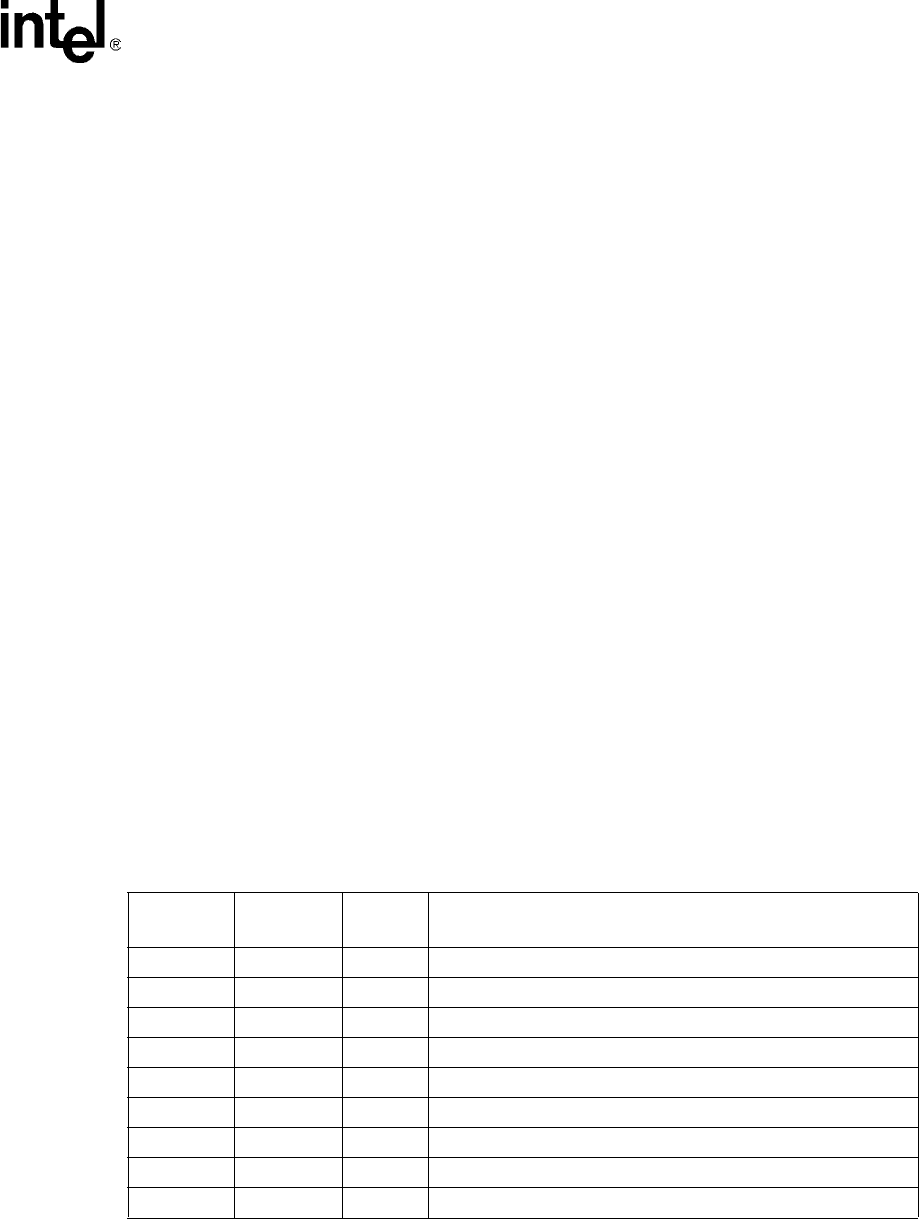
Table 73. Queue Format
Name
Longword
Number
Bit
Number
1
1. Bits 31:24 of longword number 2 are available for use by microcode.
Definition
EOP 0 31 End of Packet — decrement Q_count on dequeue
SOP 0 30 Start of Packet — used by the programmer
Cell Count 0 29:24 Number of cells in the buffer
Head 0 23:0 Head pointer
Tail 1 23:0 Tail pointer
Q_count 2 23:0 Number of packets on the queue or number of buffers on the queue
SW_Private 2 31:24 Ignored by hardware, returned to Microengine
Head Valid N/A Cached head pointer valid — maintained by hardware
Tail Valid N/A Cached tail pointer valid — maintained by hardware