Intel® Itanium® 2 Processor Intel® Itanium® 2 Processor 1.66 GHz with 9 MB L3 Cache Intel® Itanium® 2 Processor 1.66 GHz with 6 MB L3 Cache Intel® Itanium® 2 Processor 1.6 GHz with 9 MB L3 Cache Intel® Itanium® 2 Processor 1.6 GHz with 6 MB L3 Cache Intel® Itanium® 2 Processor 1.5 GHz with 6 MB L3 Cache Intel® Itanium® 2 Processor 1.5 GHz with 4 MB L3 Cache Intel® Itanium® 2 Processor 1.4 GHz with 4 MB L3 Cache Intel® Itanium® 2 Processor 1.3 GHz with 3 MB L3 Cache Intel® Itanium® 2 Processor 1.
INFORMATION IN THIS DOCUMENT IS PROVIDED IN CONNECTION WITH INTEL® PRODUCTS. NO LICENSE, EXPRESS OR IMPLIED, BY ESTOPPEL OR OTHERWISE, TO ANY INTELLECTUAL PROPERTY RIGHTS IS GRANTED BY THIS DOCUMENT.
Contents 1 Introduction....................................................................................................................... 11 1.1 1.2 1.3 1.4 1.5 1.6 2 Overview ............................................................................................................. 11 Processor Abstraction Layer ............................................................................... 11 Mixing Processors of Different Frequencies and Cache Sizes ........................... 12 Terminology...
6.2 6.3 6.4 6.5 6.6 6.7 A Signals Reference............................................................................................................ 91 A.1 4 6.1.3 SMBus Device Addressing..................................................................... 81 Processor Information ROM................................................................................ 82 Scratch EEPROM ...............................................................................................
A.2 A.1.37 ID[9:0]# (I) ..............................................................................................99 A.1.38 IDS# (I) ................................................................................................... 99 A.1.39 IGNNE# (I)............................................................................................100 A.1.40 INIT# (I) ................................................................................................100 A.1.41 INT (I) ..........................
5-2 6-1 Itanium® 2 Processor Package Thermocouple Location..................................... 77 Logical Schematic of SMBus Circuitry ................................................................ 80 2-1 2-2 2-3 2-4 2-5 2-6 2-7 2-8 2-9 2-10 2-11 2-12 2-13 Itanium® 2 Processor System Bus Signal Groups .............................................. 16 Itanium® 2 Processor Package Specifications .................................................... 17 Itanium® 2 Processor Power Supply Specifications.....
6-2 6-3 6-4 6-5 6-6 6-7 6-8 6-9 6-10 6-11 6-12 6-13 6-14 6-15 6-16 A-1 A-2 A-3 A-5 A-4 A-6 A-7 A-8 A-9 A-10 A-11 A-12 A-13 A-14 A-15 Datasheet Thermal Sensing Device SMBus Addressing on the Itanium® 2 Processor ....... 81 EEPROM SMBus Addressing on the Itanium® 2 Processor ............................... 82 Processor Information ROM Format ................................................................... 82 Current Address Read SMBus Packet ...............................................................
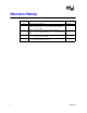
Revision History Revision No. 8 Description Date -001 Initial release of this document. July 2002 -002 Updated content to include information pertaining to Itanium 2 processor (1.5 GHz, 6 MB), Itanium 2 processor (1.4 GHz, 4 MB) and Itanium 2 processor (1.3 GHz, 3 MB). June 2003 -003 Updated content to include information pertaining to Itanium® 2 processor (1.5 GHz, 4 MB) and Itanium 2 processor (1.6 GHz, 6 MB and 9 MB).
Intel® Itanium® 2 Processor Intel® Itanium® 2 Processor 1.66 GHz with 9 MB L3 Cache Intel® Itanium® 2 Processor 1.66 GHz with 6 MB L3 Cache Intel® Itanium® 2 Processor 1.6 GHz with 9 MB L3 Cache Intel® Itanium® 2 Processor 1.6 GHz with 6 MB L3 Cache Intel® Itanium® 2 Processor 1.5 GHz with 6 MB L3 Cache Intel® Itanium® 2 Processor 1.5 GHz with 4 MB L3 Cache Intel® Itanium® 2 Processor 1.4 GHz with 4 MB L3 Cache Intel® Itanium® 2 Processor 1.3 GHz with 3 MB L3 Cache Intel® Itanium® 2 Processor 1.
Datasheet
1 Introduction 1.1 Overview The Itanium 2 processor employs Explicitly Parallel Instruction Computing (EPIC) design concepts for a tighter coupling between hardware and software. In this design style, the interface between hardware and software is designed to enable the software to exploit all available compiletime information, and efficiently deliver this information to the hardware.
Introduction 1.3 Mixing Processors of Different Frequencies and Cache Sizes All Itanium 2 processors on the same system bus are required to have the same cache size (9 MB, 6 MB, 4 MB, 3 MB or 1.5 MB) and identical core frequency. Mixing components of different core frequencies and cache sizes is not supported and has not been validated by Intel. Operating system support for multiprocessing with mixed components should also be considered.
Introduction 1.
Introduction 14 Datasheet
2 Electrical Specifications This chapter describes the electrical specifications of the Itanium 2 processor. 2.1 Itanium® 2 Processor System Bus Most Itanium 2 processor signals use the Itanium processor’s assisted gunning transceiver logic (AGTL+) signaling technology. The termination voltage, VCTERM, is generated on the baseboard and is the system bus high reference voltage.
Electrical Specifications .. Table 2-1.
Electrical Specifications 2.3 VCTERM System bus termination voltage. GND System ground. N/C No connection can be made to these pins. TERMA, TERMB The Itanium 2 processor uses two pins to control the on-die termination function, TERMA and TERMB. Both of these termination pins must be pulled to VCTERM in order to terminate the system bus using the on-die termination resistors. Both of these termination pins must be pulled to GND in order to use off-die termination.
Electrical Specifications NOTES: 1. This is the tolerance requirement, across a 200 MHz bandwidth, at the processor pins. The requirement at the processor pins accounts for voltage drops (and impedance discontinuities) at the processor pins and to the processor core. In addition to the ±1.5% DC tolerance, there is a ±3.5% AC tolerance for a total of ±5% tolerance. 2. The Itanium® 2 processor system bus is terminated at each end of the system bus.
Electrical Specifications Table 2-4. AGTL+ Signals DC Specifications (Sheet 2 of 2) Symbol Parameter IL Leakage Current CAGTL+ AGTL+ Pad Capacitance Core Frequency Minimum Typ Maximum Unit Notes All ±100 µA 5 900 MHz 3 pF 6 1.0 GHz 3 pF 6 1.3 GHz 1.5 pF 6 1.4 GHz 1.5 pF 6 1.5 GHz 1.5 pF 6 1.6 GHz 1.5 pF 6 1.66 GHz 1.5 pF 6 NOTES: 1. The typical transition point between VIL and VIH assuming 125 mV VREF uncertainty for ODT.
Electrical Specifications Table 2-8. SMBus DC Specifications Symbol Parameter Minimum Typ Maximum Unit Notes 3.3V VCC for the System Management Components 3.14 3.3 3.47 V 3.3V ±5% VIL Input Low Voltage –0.3 0.3*3.3V V VIH Input High Voltage 2.31 3.47 V VOL Output Low Voltage I3.3V 3.3V Supply Current IOL Output Low Current IOL2 Output Low Current ILI Input Leakage Current 10 µA ILO Output Leakage Current 10 µA 5.0 Max = 3.3 +5% Min + 0.7*3.3V 0.4 V 30.
Electrical Specifications Table 2-10. System Bus Clock Differential HSTL AC Specifications (Sheet 2 of 2) System Bus Clock (MHz) Minimum Typ Maximum Unit Figure Notes BCLKp Low Time 266 1.69 1.88 2.06 ns Figure 2-1 4 ns Figure 2-1 Symbol Tlow Parameter Tperiod BCLKp Period 333 Tskew System Clock Skew 333 3.0 60 ps 333 MHz Figure 2-1 50 ps Figure 2-1 3 fBCLK BCLKp Frequency 333 Tjitter BCLKp Input Jitter 333 Thigh BCLKp High Time 333 1.35 1.5 1.
Electrical Specifications Figure 2-1. Generic Clock Waveform Thigh Tlow Trise Vpp Tjitter Tfall BCLKN 80% 20% Tperiod BCLKP Trise = Rise Time Tperiod = Period Tfall = Fall Time Tjitter = Long Term Peak-to-Peak Jitter Thigh = High Time Vpp = Peak-to-Peak Swing Tlow = Low Time 000615 Figure 2-2. SMSC Clock Waveform Thigh Trise SMSC Vcc (3.3V) 90% Vcc 75% Vcc 25% Vcc Tfall Trise = Rise Time Thigh = High Time Tfall = Fall Time Tlow = Low Time Tlow 000618 2.4.
Electrical Specifications Table 2-12. Itanium® 2 Processor Absolute Maximum Ratings (Sheet 2 of 2) Symbol Parameter Minimum Maximum Unit Notes Vin, SMBus SMBus Buffer DC Input Voltage with Respect to GND –0.1 6.0 V 4 Vin, AGTL+ AGTL+ Buffer DC Input Voltage with Respect to GND –0.1 1.9 V 5, 6 VCTERM Any VCTERM Voltage with Respect to GND –0.1 1.9 V 3 Vin,TAP TAP Buffer DC Input Voltage with Respect to GND. –0.1 2.1 V 5 NOTES: 1. 2. 3. 4. 5. 6. 2.
Electrical Specifications Figure 2-3. System Bus Signal Waveform Exhibiting Overshoot/Undershoot Maximum Absolute Overshoot Time-dependent Overshoot V MAX V CTERM V REF V OL GND V MIN Maximum Absolute Undershoot Time-dependent Undershoot 000588 2.5.2 Overshoot/Undershoot Pulse Duration Pulse duration describes the total time an overshoot/undershoot event exceeds the overshoot/undershoot reference voltage (VCTERM/GND). The total time could encompass several oscillations above the reference voltage.
Electrical Specifications Note: AF for the common clock AGTL+ signals is referenced to BCLKn, and BCLKp frequency. The wired-OR Signals (BINIT#, HIT#, HITM#, BNR#, TND#, BERR#) are common clock AGTL+ signals. Note: AF for source synchronous (2x) signals is referenced to STBP#[7:0], and STBN#[7:0]. 2.5.4 Reading Overshoot/Undershoot Specification Tables The overshoot/undershoot specification for the processor is not a simple single value.
Electrical Specifications 3. If multiple overshoots and/or multiple undershoots occur, measure the worst-case pulse duration for each magnitude and compare the results against the AF = 1 specifications. If all of these worst-case overshoot or undershoot events meet the specifications (measured time < specifications) in the table (where AF = 1), then the system passes. Table 2-13.
Electrical Specifications Table 2-15. Itanium® 2 Processors (1.5 GHz/4 MB, 1.6 GHz) Source Synchronous AGTL+ Signal Group Time-Dependent Overshoot/Undershoot Tolerance for 400 MHz System Bus Absolute Maximum (V) Pulse Duration (ns) Overshoot Undershoot AF = 11 AF = 0.75 AF = 0.5 AF = 0.25 AF = 0.1 AF = 0.05 AF = 0.01 1.8 –0.6 0.0083 0.0090 0.0143 0.0287 0.0717 0.1431 0.7169 1.75 –0.55 0.0216 0.0287 0.0430 0.0861 0.2157 0.4313 2.1552 1.7 –0.5 0.0646 0.0861 0.1291 0.2584 0.
Electrical Specifications Table 2-17. Itanium® 2 Processors (1.66 GHz) Source Synchronous AGTL+ Signal Group Time-Dependent Overshoot/Undershoot Tolerance for 667 MHz System Bus Absolute Maximum (V) Overshoot Undershoot Pulse Duration (ns) AF = 11 AF = 0.75 AF = 0.5 AF = 0.25 AF = 0.1 AF = 0.05 AF = 0.01 1.8 –0.6 0.0050 0.0054 0.0086 0.0172 0.0423 0.0858 0.4297 1.75 –0.55 0.0129 0.0172 0.0258 0.0517 0.1292 0.2585 1.2953 1.7 –0.5 0.0387 0.0516 0.0775 0.1553 0.3882 0.
Electrical Specifications Table 2-19. Itanium® 2 Processors (1.5 GHz/4 MB, 1.6 GHz) Wired-OR Signal Group (BINIT#, HIT#, HITM#, BNR#, TND#, BERR#) Overshoot/Undershoot Tolerance for 400 MHz System Bus Absolute Maximum (V) Pulse Duration (ns) Overshoot Undershoot AF = 11 AF = 0.75 AF = 0.5 AF = 0.25 AF = 0.1 AF = 0.05 AF = 0.01 1.8 –0.6 0.0513 0.0685 0.1026 0.2054 0.5129 1.0258 5 1.75 –0.55 0.1547 0.2059 0.3088 0.6192 1.5458 3.0902 5 1.7 –0.5 0.4640 0.6191 0.9265 1.8536 4.
Electrical Specifications Table 2-21. Itanium® 2 (1.66 GHz) Processors Wired-OR Signal Group (BINIT#, HIT#, HITM#, BNR#, TND#, BERR#) Overshoot/Undershoot Tolerance for 667 MHz System Bus (Sheet 2 of 2) Absolute Maximum (V) Pulse Duration (ns) 1.6 –0.4 2.4567 3 3 3 3 3 3 1.55 –0.35 3 3 3 3 3 3 3 1.5 –0.3 3 3 3 3 3 3 3 NOTES: 1. Activity Factor = 1 means signal toggles every 6 ns. 2.
Electrical Specifications The power pod provides a selectable output voltage controlled via multiple binary weighted Voltage Identification (VID) inputs. The VID value (high = 1; low = 0) is defined in Table 2-23. VID pads shall be considered as LVTTL inputs to the power pod, having resistive pull-ups (5 kΩ) included inside the power pod to the internal 3.3 V power supply. The VID pads on the power connector tab will be pulled low with 10 Ω resistors that are internal to the processor.
Electrical Specifications Table 2-24. Processor Power States State Transition Ramp Rate Comment Zero to 1st Power State (A) 10 μs Off state to initial power on. 1st Power State to 2nd Power State (B) 10 μs 1st power state is defined as the system minimum operating load. Fastest power up sequence. 2nd Power State to 3rd Power State (C) 10 μs 2nd power state is defined as 75% of full power. 3rd Power State to 2nd Power State (D) 10 μs 3rd power state is defined as 40% of full power.
Electrical Specifications Listed in Table 2-25 are the system bus ratios defined for the Itanium 2 processor. The Itanium 2 processor supports bus ratios of 2/9, 2/10, 2/13, 2/14, 2/15 and 2/16. Table 2-25 lists the system bus ratios defined for the Itanium 2 processor. Each particular implementation of the Itanium 2 processor only supports a small subset of the ratios listed in Table 2-25. The supported ratios are defined below: • • • • • • The Itanium 2 processor 900 MHz with 1.
Electrical Specifications Figure 2-6. System Bus Reset and Configuration Timings for Cold Reset t-4 t-3 t-2 t-1 t0 t1 t2 t3 BCLK PWRGOOD TA RESET# TC TB TD Bus Ratio (A[21:17]#) TE Additional Configuration Signals TF TA = 1.
Electrical Specifications Figure 2-7. System Bus Reset and Configuration Timings for Warm Reset t-4 t-3 t-2 t-1 t0 t1 t2 t3 BCLK PWRGOOD TA RESET# TC TB TD Bus Ratio (A[21:17]#) TE Additional Configuration Signals TF TA = 1.
Electrical Specifications Table 2-26. Connection for Unused Pins (Sheet 2 of 2) Pins/Pin Groups Recommended Connections Notes System Management Signals 3.3V GND SMA[2:0] N/C SMSC N/C SMSD N/C SMWP N/C THRMALERT# H 1, 4 LVTTL Power Pod Signals OUTEN Must be used PPODGD# Must be used CPUPRES# Must be used Reserved Pins N/C N/C NOTES: 1. 2. 3. 4. 36 L = GND, H = VCTERM. AGTL+ output signals SBSY[0:1]#, DBSY[0:1]#, and DRDY[0,1]# may be left as N/C if not used on platform.
3 Pinout Specifications This chapter describes the Itanium 2 processor signals and pinout. Note: The pins labeled “N/C” must remain unconnected. The Itanium 2 processor uses a JEDEC standard pin naming convention. In this chapter, pin names are the actual names given to each physical pin of the processor. System bus signal names are the names associated with the functions of those pins.
Pinout Specifications Table 3-1 provides the Itanium 2 processor pin list in alphabetical order. Table 3-2 provides the Itanium 2 processor pin list by pin location. Table 3-1. Pin/Signal Information Sorted by Pin Name (Sheet 1 of 15) Pin Name System Bus Signal Name 3.
Pinout Specifications Table 3-1.
Pinout Specifications Table 3-1.
Pinout Specifications Table 3-1.
Pinout Specifications Table 3-1.
Pinout Specifications Table 3-1.
Pinout Specifications Table 3-1.
Pinout Specifications Table 3-1.
Pinout Specifications Table 3-1.
Pinout Specifications Table 3-1.
Pinout Specifications Table 3-1.
Pinout Specifications Table 3-1.
Pinout Specifications Table 3-1.
Pinout Specifications Table 3-1.
Pinout Specifications Table 3-1.
Pinout Specifications Table 3-2.
Pinout Specifications Table 3-2.
Pinout Specifications Table 3-2.
Pinout Specifications Table 3-2.
Pinout Specifications Table 3-2.
Pinout Specifications Table 3-2.
Pinout Specifications Table 3-2.
Pinout Specifications Table 3-2.
Pinout Specifications Table 3-2.
Pinout Specifications Table 3-2.
Pinout Specifications Table 3-2.
Pinout Specifications Table 3-2.
Pinout Specifications Table 3-2.
Pinout Specifications Table 3-2.
Pinout Specifications Table 3-2.
Pinout Specifications 68 Datasheet
4 Mechanical Specifications This chapter provides the mechanical specifications of the Itanium 2 processor. 4.1 Mechanical Dimensions The Itanium 2 processor package is comprised of an interposer, a processor package substrate, and an integrated heat spreader (IHS), as illustrated in Figure 4-1. The interposer interfaces with the socket and the power pod and contains 611 pins which are positioned in a 25 x 28 grid.
Mechanical Specifications Figure 4-2. Itanium® 2 Processor Package 90.00 42.50 38.50 48.26 42.50 38.50 Top View Integrated Heat Spreader IHS Height (See Note) Processor Package Substrate Substrate Height (See Note) Interposer 1.43 0.00 2.03 Pins Side View 34.29 28 x 1.27 Pitch 25 x 1.27 Pitch 611 x Ø 0.305 Pins 30.48 Bottom View All dimensions are measured in mm. Not to scale. 000655g NOTE: Processor 70 IHS Height Substrate Height Units 900 MHz (1.5 MB) 5.575 3.397 mm 1.
Mechanical Specifications Figure 4-3. Itanium® 2 Processor Package Power Tab CL 2.48 2x R1.20 12x 2.92 2x 25.85 24.13 12x 0.86 10x 1.15 46.96 CL 46.74 2x 16.10 12x 38.76 42.46 48.26 45.00 90.00 Top View CL 2.98 2x 9.10 2x 12.91 46.96 46.00 42.21 4x R1.00 Bottom View All dimensions are measured in mm. Not to scale.
Mechanical Specifications 4.2 Package Marking The following section details the processor top-side and bottom-side markings for the Itanium 2 processor and is provided as an identification aid. The processor top-side mark for the product is a laser marking on the IHS. 4.2.1 Processor Top-Side Marking Figure 4-4 shows an example of the laser marking on the IHS.
Mechanical Specifications Figure 4-5. Processor Bottom-Side Marking Placement on Interposer Laser Mark including 2D Matrix Mark AH25 A25 AH1 A1 Pin 1 Indicator 001267b NOTE: 2D Matrix Mark only present on Itanium 2 processor (6 MB), Itanium 2 processor (4 MB) and Itanium 2 processor (1.3 GHz, 3 MB).
Mechanical Specifications 74 Datasheet
5 Thermal Specifications This chapter provides a description of the thermal features relating to the Itanium 2 processor. 5.1 Thermal Features The Itanium 2 processor has an internal thermal circuit which senses when a certain temperature is reached on the processor core. This circuit is used for controlling various thermal states. In addition, an on-chip thermal diode is available for use by the thermal sensing device on the Itanium 2 processor.
Thermal Specifications 5.1.2 Enhanced Thermal Management ETM is a new feature that has been added to the Itanium 2 processor. ETM uses a thermal sensing device on the die to monitor a thermal entry point, indicating dangerous operation exceeding the thermal specification. Once the thermal sensing device observes the temperature rise above the thermal entry point, the processor will enter a low power mode of execution and notify the system by sending a Correctable Machine Check Interrupt (CMCI).
Thermal Specifications Figure 5-2. Itanium® 2 Processor Package Thermocouple Location 24.13 45.00 Thermocouple Location All dimensions are measured in mm. Not to scale.
Thermal Specifications 78 Datasheet
6 System Management Feature Specifications The Itanium 2 processor includes a system management bus (SMBus) interface. This chapter describes the features of the SMBus and SMBus components. 6.1 System Management Bus 6.1.1 System Management Bus Interface The Itanium 2 processor includes an Itanium processor family SMBus interface which allows access to several processor features.
System Management Feature Specifications Figure 6-1. Logical Schematic of SMBus Circuitry Intel® Itanium ® 2 Processor 3.3V Core 10K 10K THERMDA 10K VCC THERMDC A0 A1 A2 Processor SC Information SD ROM VCC A0 A1 STBY Thermal Sensing Device SC SD 10K ALERT VCC A0 A1 10K A2 SC Scratch EEPROM SD WP 10K SMA0 3.3V SMWP SMA1 SMA2 SMSD SMSC THRMALERT# 3.3V 3.3V 10K Stuffing Options System Board System Board NOTE: 1. Actual implementation may vary. 2.
System Management Feature Specifications 6.1.3 SMBus Device Addressing Of the addresses broadcast across the SMBus, the memory components claim those of the form “1010XXYZb”. The “XX” and “Y” bits are used to enable the devices on the processor at adjacent addresses. The Y bit is hard-wired on the processor to GND (‘0’) for the Scratch EEPROM and pulled to 3.3V (‘1’) for the processor information ROM.
System Management Feature Specifications Table 6-3.
System Management Feature Specifications Table 6-4. Processor Information ROM Format (Sheet 2 of 4) Offset/ Section 09h # of Bits Function Notes Byte pointer, 00h if not present Examples 8 Feature Data Address 67h 0Ah 8 Other Data Address Byte pointer, 00h if not present 7Ah 0Bh 16 Reserved Reserved for future use 0000h 0Dh 8 Checksum 1 byte checksum Add up by byte and take 2’s complement.
System Management Feature Specifications Table 6-4. Processor Information ROM Format (Sheet 3 of 4) Offset/ Section # of Bits Function Notes Examples Package 37h 32 Package Revision Four 8-bit ASCII characters Itanium® 2 Package = INT2b, (1.
System Management Feature Specifications Table 6-4. Processor Information ROM Format (Sheet 4 of 4) Offset/ Section # of Bits Function Notes Examples 1 indicates EEPROM data for specified field is valid.
System Management Feature Specifications controller continues to transmit data bytes until it terminates the sequence with a stop. All data bytes will result in an acknowledge from the Scratch EEPROM. If more than eight bytes are written, the internal address will “roll over” and the previous data will be overwritten.
System Management Feature Specifications THRMALERT# signal (see Section 6.1.1 for more details). At power up, the appropriate alarm register values need to be programmed into the thermal sensing device via the SMBus. It is recommended that the upper thermal reference threshold byte (provided in the processor information ROM) be used for setting the upper threshold value in the alarm register.
System Management Feature Specifications Table 6-13. Command Byte Bit Assignment Register Command Reset State Function RESERVED 00h N/A RRT 01h N/A Read processor core thermal data. RS 02h N/A Read status byte (flags, busy signal). RC 03h 0000 0000 Read configuration byte. RCR 04h 0000 0010 Read conversion rate byte. RESERVED 05h 0111 1111 Reserved for future use. RESERVED 06h 1100 1001 Reserved for future use. Read processor core thermal diode THIGH limit.
System Management Feature Specifications 6.7.2 Thermal Limit Registers The thermal sensing device has two thermal limit registers; they define high and low limits for the processor core thermal diode. The encoding for these registers is the same as for the thermal reference registers. If the diode thermal value equals or exceeds one of its limits, then its alarm bit in the status register is triggered. This indication is also brought out to the Itanium 2 processor system bus via the THRMALERT# signal. 6.
System Management Feature Specifications 6.7.5 Conversion Rate Register The contents of the conversion rate register determine the nominal rate at which analog-to-digital conversions happen when the thermal sensing device is in auto-convert mode. Table 6-16 shows the mapping between conversion rate register values and the conversion rate. As indicated in Table 6-16, the conversion rate register is set to its default state of 02h (0.25 Hz nominally) when the thermal sensing device is powered-up.
A Signals Reference This appendix provides an alphabetical listing of all Itanium 2 processor system bus signals. The tables at the end of this appendix summarize the signals by direction: output, input, and I/O. For a complete pinout listing including processor specific pins, please refer to Chapter 3, “Pinout Specifications.” A.1 Alphabetical Signals Reference A.1.1 A[49:3]# (I/O) The Address (A[49:3]#) signals, with byte enables, define a 250 Byte physical memory address space.
Signals Reference Table A-1. Address Space Size ASZ[1:0]# Memory Address Space Memory Access Range 0 0 Reserved Reserved 0 1 36-bit 0 to (64 GByte - 1) 1 0 50-bit 64 GByte to (1 Pbyte –1) 1 1 Reserved Reserved Any memory access transaction addressing a memory region that is less than 64 GB (that is, Aa[49:36]# are all zeroes) must set ASZ[1:0]# to 01.
Signals Reference For memory or I/O transactions, the byte-enable signals indicate that valid data is requested or being transferred on the corresponding byte on the 128-bit data bus. BE[0]# indicates that the least significant byte is valid, and BE[7]# indicates that the most significant byte is valid. Since BE[7:0]# specifies the validity of only 8 bytes on the 16 byte wide bus, A[3]# is used to determine which half of the data bus is validated by BE[7:0]#.
Signals Reference A.1.10 BINIT# (I/O) If enabled by configuration, the Bus Initialization (BINIT#) signal is asserted to signal any bus condition that prevents reliable future operation. If BINIT# observation is enabled during power-on configuration, and BINIT# is sampled asserted, all bus state machines are reset. All agents reset their rotating IDs for bus arbitration to the same state as that after reset, and internal count information is lost. The L2 and L3 caches are not affected.
Signals Reference Table A-4. BR0# (I/O), BR1#, BR2#, BR3# Signals for 4P Rotating Interconnect Bus Signal Agent 0 Pins Agent 1 Pins Agent 2 Pins Agent 3 Pins BREQ[0]# BR[0]# BR[3]# BR[2]# BR[1]# BREQ[1]# BR[1]# BR[0]# BR[3]# BR[2]# BREQ[2]# BR[2]# BR[1]# BR[0]# BR[3]# BREQ[3]# BR[3]# BR[2]# BR[1]# BR[0]# Table A-5.
Signals Reference sampling BREQn# asserted by another symmetric agent, the symmetric owner deasserts BREQn# as soon as possible to release the bus. A symmetric owner stops issuing new requests that are not part of an existing locked operation on observing BPRI# asserted. A symmetric agent can deassert BREQn# before it becomes a symmetric owner. A symmetric agent can reassert BREQn# after keeping it deasserted for one clock. A.1.16 CCL# (I/O) CCL# is the Cache Cleanse signal.
Signals Reference A.1.22 DBSY_C2# (O) DBSY# is a copy of the Data Bus Busy signal. This copy of the Data Bus Busy signal (DBSY_C2#) is an output only. A.1.23 DEFER# (I) The DEFER# signal is asserted by an agent to indicate that the transaction cannot be guaranteed inorder completion. Assertion of DEFER# is normally the responsibility of the priority agent. A.1.24 DEN# (I/O) The Defer Enable (DEN#) signal is driven on the bus on the second clock of the Request Phase on the Ab[4]# pin.
Signals Reference The Deferred Reply agent transmits the DID[9:0]# (Ab[25:16]#) signals received during the original transaction on the Aa[25:16]# signals during the Deferred Reply transaction. This process enables the original requesting agent to make an identifier match with the original request that is awaiting completion. A.1.27 DPS# (I/O) The Deferred Phase Enable (DPS#) signal is driven to the bus on the second clock of the Request Phase on the Ab[3]# pin.
Signals Reference Table A-8. Extended Function Signals Extended Function Signal A.1.33 Signal Name Alias Function EXF[4]# Reserved Reserved EXF[3]# SPLCK#/FCL# Split Lock / Flush Cache Line EXF[2]# OWN#/CCL# Memory Update Not Needed / Cache Cleanse EXF[1]# DEN# Defer Enable EXF[0]# DPS# Deferred Phase Supported FCL# (I/O) The Flush Cache Line (FCL#) signal is driven to the bus on the second clock of the Request Phase on the A[6]# pin.
Signals Reference A.1.39 IGNNE# (I) IGNNE# is ignored in the Itanium 2 processor system environment. A.1.40 INIT# (I) The Initialization (INIT#) signal triggers an unmasked interrupt to the processor. INIT# is usually used to break into hanging or idle processor states. Semantics required for platform compatibility are supplied in the PAL firmware interrupt service routine. A.1.41 INT (I) INT is the 8259-compatible Interrupt Request signal which indicates that an external interrupt has been generated.
Signals Reference A.1.44 LINT[1:0] (I) LINT[1:0] are local interrupt signals. These pins are disabled after RESET#. LINT[0] is typically software configured as INT, an 8259-compatible maskable interrupt request signal. LINT[1] is typically software configured as NMI, a non-maskable interrupt.Both signals are asynchronous inputs. A.1.45 LOCK# (I/O) LOCK# is never asserted or sampled in the Itanium 2 processor system environment. A.1.46 NMI (I) The NMI signal is the Non-maskable Interrupt signal.
Signals Reference All receiving agents observe the REQ[5:0]# signals to determine the transaction type and participate in the transaction as necessary, as shown in Table A-10. Table A-10. Transaction Types Defined by REQa#/REQb# Signals REQa[5:0]# REQb[5:0]# Transaction A.1.
Signals Reference A correct parity signal is high if an even number of covered signals are low and low if an odd number of covered signals are low. This definition allows parity to be high when all covered signals are high. A.1.53 RS[2:0]# (I) The Response Status (RS[2:0]#) signals are driven by the responding agent (the agent responsible for completion of the transaction). A.1.
Signals Reference A.1.59 STBn[7:0]# and STBp[7:0]# (I/O) STBp[7:0]# and STBn[7:0]# (and DRDY#) are used to transfer data at the 2x transfer rate in lieu of BCLKp. They are driven by the data transfer agent with a tight skew relationship with respect to its corresponding bus signals, and are used by the receiving agent to capture valid data in its latches. This functions like an independent double frequency clock constructed from a falling edge of either STBp[7:0]# or STBn[7:0]#.
Signals Reference A.1.64 THRMALERT# (O) THRMALERT# is asserted when the measured temperature from the processor thermal diode equals or exceeds the temperature threshold data programmed in the high-temp (THIGH) or lowtemp (TLOW) registers on the sensor. This signal can be used by the platform to implement thermal regulation features. A.1.65 TMS (I) The Test Mode Select (TMS) signal is an IEEE 1149.1 compliant TAP specification support signal used by debug tools. A.1.
Signals Reference Table A-12.
Signals Reference Table A-14.
Signals Reference 108 Datasheet