
Desktop 4th Generation Specification Sheet
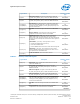
Table Of Contents
- Contents
- Revision History
- 1.0 Introduction
- 2.0 Interfaces
- 3.0 Technologies
- 3.1 Intel® Virtualization Technology (Intel® VT)
- 3.2 Intel® Trusted Execution Technology (Intel® TXT)
- 3.3 Intel® Hyper-Threading Technology (Intel® HT Technology)
- 3.4 Intel® Turbo Boost Technology 2.0
- 3.5 Intel® Advanced Vector Extensions 2.0 (Intel® AVX2)
- 3.6 Intel® Advanced Encryption Standard New Instructions (Intel® AES-NI)
- 3.7 Intel® Transactional Synchronization Extensions - New Instructions (Intel® TSX-NI)
- 3.8 Intel® 64 Architecture x2APIC
- 3.9 Power Aware Interrupt Routing (PAIR)
- 3.10 Execute Disable Bit
- 3.11 Supervisor Mode Execution Protection (SMEP)
- 4.0 Power Management
- 4.1 Advanced Configuration and Power Interface (ACPI) States Supported
- 4.2 Processor Core Power Management
- 4.3 Integrated Memory Controller (IMC) Power Management
- 4.4 PCI Express* Power Management
- 4.5 Direct Media Interface (DMI) Power Management
- 4.6 Graphics Power Management
- 5.0 Thermal Management
- 5.1 Desktop Processor Thermal Profiles
- 5.2 Thermal Metrology
- 5.3 Fan Speed Control Scheme with Digital Thermal Sensor (DTS) 1.1
- 5.4 Fan Speed Control Scheme with Digital Thermal Sensor (DTS) 2.0
- 5.5 Processor Temperature
- 5.6 Adaptive Thermal Monitor
- 5.7 THERMTRIP# Signal
- 5.8 Digital Thermal Sensor
- 5.9 Intel® Turbo Boost Technology Thermal Considerations
- 6.0 Signal Description
- 6.1 System Memory Interface Signals
- 6.2 Memory Reference and Compensation Signals
- 6.3 Reset and Miscellaneous Signals
- 6.4 PCI Express*-Based Interface Signals
- 6.5 Display Interface Signals
- 6.6 Direct Media Interface (DMI)
- 6.7 Phase Locked Loop (PLL) Signals
- 6.8 Testability Signals
- 6.9 Error and Thermal Protection Signals
- 6.10 Power Sequencing Signals
- 6.11 Processor Power Signals
- 6.12 Sense Signals
- 6.13 Ground and Non-Critical to Function (NCTF) Signals
- 6.14 Processor Internal Pull-Up / Pull-Down Terminations
- 7.0 Electrical Specifications
- 8.0 Package Mechanical Specifications
- 9.0 Processor Ball and Signal Information

Reset and Miscellaneous Signals
Table 33. Reset and Miscellaneous Signals
Signal Name Description Direction /
Buffer Type
CFG[19:0]
Configuration Signals: The CFG signals have a default value of
'1' if not terminated on the board.
• CFG[1:0]: Reserved configuration lane. A test point may be
placed on the board for these lanes.
• CFG[2]: PCI Express* Static x16 Lane Numbering Reversal.
— 1 = Normal operation
— 0 = Lane numbers reversed.
• CFG[3]: MSR Privacy Bit Feature
— 1 = Debug capability is determined by
IA32_Debug_Interface_MSR (C80h) bit[0] setting
— 0 = IA32_Debug_Interface_MSR (C80h) bit[0] default
setting overridden
• CFG[4]: Reserved configuration lane. A test point may be
placed on the board for this lane.
• CFG[6:5]: PCI Express* Bifurcation:
1
— 00 = 1 x8, 2 x4 PCI Express*
— 01 = reserved
— 10 = 2 x8 PCI Express*
— 11 = 1 x16 PCI Express*
• CFG[19:7]: Reserved configuration lanes. A test point may
be placed on the board for these lands.
I/O
GTL
CFG_RCOMP
Configuration resistance compensation. Use a 49.9 Ω ±1%
resistor to ground.
—
FC_x
FC (Future Compatibility) signals are signals that are available for
compatibility with other processors. A test point may be placed
on the board for these lands.
PM_SYNC
Power Management Sync: A sideband signal to communicate
power management status from the platform to the processor.
I
CMOS
PWR_DEBUG#
Signal is for debug. I
Asynchronous
CMOS
IST_TRIGGER
Signal is for IFDIM testing only. I
CMOS
IVR_ERROR
Signal is for debug. If both THERMTRIP# and this signal are
simultaneously asserted, the processor has encountered an
unrecoverable power delivery fault and has engaged automatic
shutdown as a result.
O
CMOS
RESET#
Platform Reset pin driven by the PCH. I
CMOS
RSVD
RSVD_TP
RSVD_NCTF
RESERVED: All signals that are RSVD and RSVD_NCTF must be
left unconnected on the board. Intel recommends that all
RSVD_TP signals have via test points.
No Connect
Test Point
Non-Critical to
Function
SM_DRAMRST#
DRAM Reset: Reset signal from processor to DRAM devices. One
signal common to all channels.
O
CMOS
TESTLO_x
TESTLO should be individually connected to V
SS
through a
resistor.
Note: 1. PCIe bifurcation support varies with the processor and PCH SKUs used.
6.3
Signal Description—Processor
Desktop 4th Generation Intel
®
Core
™
Processor Family, Desktop Intel
®
Pentium
®
Processor Family, and Desktop Intel
®
Celeron
®
Processor Family
December 2013 Datasheet – Volume 1 of 2
Order No.: 328897-004 85