
Desktop 4th Generation Specification Sheet
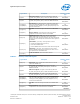
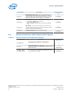
Table Of Contents
- Contents
- Revision History
- 1.0 Introduction
- 2.0 Interfaces
- 3.0 Technologies
- 3.1 Intel® Virtualization Technology (Intel® VT)
- 3.2 Intel® Trusted Execution Technology (Intel® TXT)
- 3.3 Intel® Hyper-Threading Technology (Intel® HT Technology)
- 3.4 Intel® Turbo Boost Technology 2.0
- 3.5 Intel® Advanced Vector Extensions 2.0 (Intel® AVX2)
- 3.6 Intel® Advanced Encryption Standard New Instructions (Intel® AES-NI)
- 3.7 Intel® Transactional Synchronization Extensions - New Instructions (Intel® TSX-NI)
- 3.8 Intel® 64 Architecture x2APIC
- 3.9 Power Aware Interrupt Routing (PAIR)
- 3.10 Execute Disable Bit
- 3.11 Supervisor Mode Execution Protection (SMEP)
- 4.0 Power Management
- 4.1 Advanced Configuration and Power Interface (ACPI) States Supported
- 4.2 Processor Core Power Management
- 4.3 Integrated Memory Controller (IMC) Power Management
- 4.4 PCI Express* Power Management
- 4.5 Direct Media Interface (DMI) Power Management
- 4.6 Graphics Power Management
- 5.0 Thermal Management
- 5.1 Desktop Processor Thermal Profiles
- 5.2 Thermal Metrology
- 5.3 Fan Speed Control Scheme with Digital Thermal Sensor (DTS) 1.1
- 5.4 Fan Speed Control Scheme with Digital Thermal Sensor (DTS) 2.0
- 5.5 Processor Temperature
- 5.6 Adaptive Thermal Monitor
- 5.7 THERMTRIP# Signal
- 5.8 Digital Thermal Sensor
- 5.9 Intel® Turbo Boost Technology Thermal Considerations
- 6.0 Signal Description
- 6.1 System Memory Interface Signals
- 6.2 Memory Reference and Compensation Signals
- 6.3 Reset and Miscellaneous Signals
- 6.4 PCI Express*-Based Interface Signals
- 6.5 Display Interface Signals
- 6.6 Direct Media Interface (DMI)
- 6.7 Phase Locked Loop (PLL) Signals
- 6.8 Testability Signals
- 6.9 Error and Thermal Protection Signals
- 6.10 Power Sequencing Signals
- 6.11 Processor Power Signals
- 6.12 Sense Signals
- 6.13 Ground and Non-Critical to Function (NCTF) Signals
- 6.14 Processor Internal Pull-Up / Pull-Down Terminations
- 7.0 Electrical Specifications
- 8.0 Package Mechanical Specifications
- 9.0 Processor Ball and Signal Information
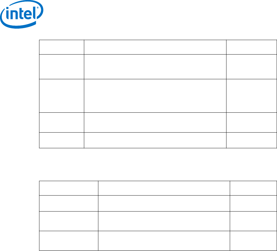
Signal Name Description Direction / Buffer
Type
SB_CK[3:0]
SDRAM Differential Clock: Channel B SDRAM Differential
clock signal pair. The crossing of the positive edge of SB_CK
and the negative edge of its complement SB_CK# are used to
sample the command and control signals on the SDRAM.
O
DDR3/DDR3L
SB_CKE[3:0]
Clock Enable: (1 per rank). These signals are used to:
• Initialize the SDRAMs during power-up.
• Power-down SDRAM ranks.
• Place all SDRAM ranks into and out of self-refresh during
STR.
O
DDR3/DDR3L
SB_CS#[3:0]
Chip Select: (1 per rank). These signals are used to select
particular SDRAM components during the active state. There is
one Chip Select for each SDRAM rank.
O
DDR3/DDR3L
SB_ODT[3:0]
On Die Termination: Active Termination Control. O
DDR3/DDR3L
Memory Reference and Compensation Signals
Table 32. Memory Reference and Compensation Signals
Signal Name Description Direction /
Buffer Type
SM_RCOMP[2:0]
System Memory Impedance Compensation: I
A
SM_VREF
DDR3/DDR3L Reference Voltage: This signal is used as
a reference voltage to the DDR3/DDR3L controller and is
defined as V
DDQ
/2
O
DDR3/DDR3L
SA_DIMM_VREFDQ
SB_DIMM_VREFDQ
Memory Channel A/B DIMM DQ Voltage Reference:
The output pins are connected to the DIMMs, and holds
V
DDQ
/2 as reference voltage.
O
DDR3/DDR3L
6.2
Processor—Signal Description
Desktop 4th Generation Intel
®
Core
™
Processor Family, Desktop Intel
®
Pentium
®
Processor Family, and Desktop Intel
®
Celeron
®
Processor Family
Datasheet – Volume 1 of 2 December 2013
84 Order No.: 328897-004