
Desktop 4th Generation Specification Sheet
Table Of Contents
- Contents
- Revision History
- 1.0 Introduction
- 2.0 Interfaces
- 3.0 Technologies
- 3.1 Intel® Virtualization Technology (Intel® VT)
- 3.2 Intel® Trusted Execution Technology (Intel® TXT)
- 3.3 Intel® Hyper-Threading Technology (Intel® HT Technology)
- 3.4 Intel® Turbo Boost Technology 2.0
- 3.5 Intel® Advanced Vector Extensions 2.0 (Intel® AVX2)
- 3.6 Intel® Advanced Encryption Standard New Instructions (Intel® AES-NI)
- 3.7 Intel® Transactional Synchronization Extensions - New Instructions (Intel® TSX-NI)
- 3.8 Intel® 64 Architecture x2APIC
- 3.9 Power Aware Interrupt Routing (PAIR)
- 3.10 Execute Disable Bit
- 3.11 Supervisor Mode Execution Protection (SMEP)
- 4.0 Power Management
- 4.1 Advanced Configuration and Power Interface (ACPI) States Supported
- 4.2 Processor Core Power Management
- 4.3 Integrated Memory Controller (IMC) Power Management
- 4.4 PCI Express* Power Management
- 4.5 Direct Media Interface (DMI) Power Management
- 4.6 Graphics Power Management
- 5.0 Thermal Management
- 5.1 Desktop Processor Thermal Profiles
- 5.2 Thermal Metrology
- 5.3 Fan Speed Control Scheme with Digital Thermal Sensor (DTS) 1.1
- 5.4 Fan Speed Control Scheme with Digital Thermal Sensor (DTS) 2.0
- 5.5 Processor Temperature
- 5.6 Adaptive Thermal Monitor
- 5.7 THERMTRIP# Signal
- 5.8 Digital Thermal Sensor
- 5.9 Intel® Turbo Boost Technology Thermal Considerations
- 6.0 Signal Description
- 6.1 System Memory Interface Signals
- 6.2 Memory Reference and Compensation Signals
- 6.3 Reset and Miscellaneous Signals
- 6.4 PCI Express*-Based Interface Signals
- 6.5 Display Interface Signals
- 6.6 Direct Media Interface (DMI)
- 6.7 Phase Locked Loop (PLL) Signals
- 6.8 Testability Signals
- 6.9 Error and Thermal Protection Signals
- 6.10 Power Sequencing Signals
- 6.11 Processor Power Signals
- 6.12 Sense Signals
- 6.13 Ground and Non-Critical to Function (NCTF) Signals
- 6.14 Processor Internal Pull-Up / Pull-Down Terminations
- 7.0 Electrical Specifications
- 8.0 Package Mechanical Specifications
- 9.0 Processor Ball and Signal Information
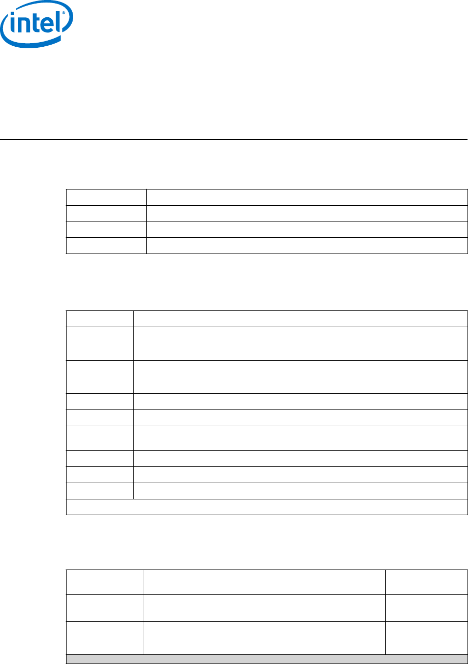
6.0 Signal Description
This chapter describes the processor signals. The signals are arranged in functional
groups according to the associated interface or category. The following notations are
used to describe the signal type.
Notation
Signal Type
I Input pin
O Output pin
I/O Bi-directional Input/Output pin
The signal description also includes the type of buffer used for the particular signal
(see the following table).
Table 29. Signal Description Buffer Types
Signal Description
PCI Express*
PCI Express* interface signals. These signals are compatible with PCI Express 3.0
Signaling Environment AC Specifications and are AC coupled. The buffers are not 3.3 V-
tolerant. See the PCI Express Base Specification 3.0.
DMI
Direct Media Interface signals. These signals are compatible with PCI Express 2.0
Signaling Environment AC Specifications, but are DC coupled. The buffers are not 3.3 V-
tolerant.
CMOS CMOS buffers. 1.05V- tolerant
DDR3/DDR3L DDR3/DDR3L buffers: 1.5 V- tolerant
A
Analog reference or output. May be used as a threshold voltage or for buffer
compensation
GTL Gunning Transceiver Logic signaling technology
Ref Voltage reference signal
Asynchronous
1
Signal has no timing relationship with any reference clock.
1. Qualifier for a buffer type.
System Memory Interface Signals
Table 30. Memory Channel A Signals
Signal Name Description Direction / Buffer
Type
SA_BS[2:0]
Bank Select: These signals define which banks are selected
within each SDRAM rank.
O
DDR3/DDR3L
SA_WE#
Write Enable Control Signal: This signal is used with
SA_RAS# and SA_CAS# (along with SA_CS#) to define the
SDRAM Commands.
O
DDR3/DDR3L
continued...
6.1
Processor—Signal Description
Desktop 4th Generation Intel
®
Core
™
Processor Family, Desktop Intel
®
Pentium
®
Processor Family, and Desktop Intel
®
Celeron
®
Processor Family
Datasheet – Volume 1 of 2 December 2013
82 Order No.: 328897-004