Desktop 3rd Generation Intel® Core™ Processor Family, Desktop Intel® Pentium® Processor Family, and Desktop Intel® Celeron® Processor Family Datasheet – Volume 1 of 2 November 2013 Document Number: 326764-008
INFORMATION IN THIS DOCUMENT IS PROVIDED IN CONNECTION WITH INTEL PRODUCTS. NO LICENSE, EXPRESS OR IMPLIED, BY ESTOPPEL OR OTHERWISE, TO ANY INTELLECTUAL PROPERTY RIGHTS IS GRANTED BY THIS DOCUMENT.
Contents 1 Introduction .............................................................................................................. 9 1.1 Processor Feature Details ................................................................................... 11 1.1.1 Supported Technologies .......................................................................... 11 1.2 Interfaces ........................................................................................................ 11 1.2.
2.4.1 2.5 2.6 3D and Video Engines for Graphics Processing ............................................33 2.4.1.1 3D Engine Execution Units ..........................................................33 2.4.1.2 3D Pipeline ...............................................................................34 2.4.1.3 Video Engine ............................................................................34 2.4.1.4 2D Engine ................................................................................35 2.4.
4.2.4 4.3 4.4 4.5 4.6 4.7 Core C-states ........................................................................................ 52 4.2.4.1 Core C0 State........................................................................... 52 4.2.4.2 Core C1 / C1E State .................................................................. 53 4.2.4.3 Core C3 State........................................................................... 53 4.2.4.4 Core C6 State......................................................
7.7 7.8 7.9 7.10 7.11 Signal Groups ...................................................................................................80 Test Access Port (TAP) Connection .......................................................................82 Storage Conditions Specifications.........................................................................83 DC Specifications ...............................................................................................84 7.10.
6-2 6-3 6-4 6-5 6-6 6-7 6-8 6-9 6-10 6-11 6-12 6-13 6-14 6-15 6-16 7-1 7-2 7-3 7-4 7-5 7-6 7-7 7-8 7-9 7-10 8-1 9-1 9-2 Memory Channel A Signals ...................................................................................... 66 Memory Channel B Signals ...................................................................................... 67 Memory Reference and Compensation....................................................................... 67 Reset and Miscellaneous Signals...................
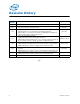
Revision History Revision Number Description Revision Date 001 • Initial release April 2012 002 • Added Desktop 3rd Generation Intel® Core™ i5-3470T, i5-3470, i5-3470S, i5-3475S, i5-3570, i5-3570S processors June 2012 • Updated Section 1.2.2, PCI Express* 003 • Updated Section 2.1.1, System Memory Technology Supported • Updated Table 7-4, “Processor Core Active and Idle Mode DC Voltage and Current Specifications”. Added 65 W to 2011C.
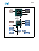
Introduction 1 Introduction The Desktop 3rd Generation Intel® Core™ processor family, Desktop Intel® Pentium® processor family, and Desktop Intel® Celeron® processor family are the next generation of 64-bit, multi-core processors built on 22-nanometer process technology. The processors are designed for a two-chip platform. The two-chip platform consists of a processor and a Platform Controller Hub (PCH) and enables higher performance, lower cost, easier validation, and improved x-y footprint.
Introduction Figure 1-1. Desktop Processor Platform PCI Express* 3.0 1 x16 or 2x8 DDR3 Discrete Graphics (PEG) Intel® Processor PECI Intel® Flexible Display Interface DMI2 x4 Serial ATA Intel® Management Engine Digital Display x 3 USB 2.0 / USB 3.01 Intel® 6/7 Series Chipset Families Intel® HD Audio Analog CRT SPI Flash x 2 SMBUS 2.0 SPI Controller Link 1 FWH PCI Express* WiFi / WiMax LPC 8 PCI Express* 2.0 x1 Ports (5 GT/s) Super I/O Gigabit Network Connection GPIO Note: 1. USB 3.
Introduction 1.1 Processor Feature Details • • • • 1.1.
Introduction • Support memory configurations that mix DDR3 DIMMs/DRAMs with DDR3L DIMMs/DRAMs running at 1.5 V • The type of the DIMM modules supported by the processor is dependent on the PCH SKU in the target platform: — Desktop PCH platforms support non-ECC UDIMMs only — All In One platforms (AIO) support SO-DIMMs • Theoretical Maximum Memory Bandwidth: — 10.6 GB/s in single-channel mode or 21.3 GB/s in dual-channel mode assuming DDR3 1333 MT/s — 12.8 GB/s in single-channel mode or 25.
Introduction to transmit data across this interface. This also does not account for packet overhead and link maintenance. • Maximum theoretical bandwidth on the interface of 8 GB/s in each direction simultaneously, for an aggregate of 16 GB/s when x16 Gen 2 • Gen 3 raw bit-rate on the data pins of 8.0 GT/s, resulting in a real bandwidth per pair of 984 MB/s using 128b/130b encoding to transmit data across this interface. This also does not account for packet overhead and link maintenance.
Introduction 1.2.3 Direct Media Interface (DMI) • DMI 2.0 support • Four lanes in each direction • 5 GT/s point-to-point DMI interface to PCH is supported • Raw bit-rate on the data pins of 5.0 Gb/s, resulting in a real bandwidth per pair of 500 MB/s given the 8b/10b encoding used to transmit data across this interface. Does not account for packet overhead and link maintenance.
Introduction • DirectX* Video Acceleration (DXVA) support for accelerating video processing — Full AVC/VC1/MPEG2 HW Decode • Advanced Scheduler 2.0, 1.0, XPDM support • Windows* 7, Windows* XP, OSX, Linux OS Support • DirectX* 11, DirectX* 10.1, DirectX* 10, DirectX* 9 support • OpenGL* 3.0 support • Switchable Graphics support on Desktop AIO platforms with MxM solutions only 1.2.
Introduction 1.3.5 Direct Media Interface (DMI) • L0s and L1 ASPM power management capability 1.3.6 Processor Graphics Controller (GT) • • • • 1.3.
Introduction Table 1-1. 1.5 Desktop 3rd Generation Intel® Core™ Processor Family, Desktop Intel® Pentium® Processor Family, and Desktop Intel® Celeron® Processor Family SKUs (Sheet 2 of 2) Processor Number TDP (W) IA LFM Frequency IA Frequency range GT Frequency range TjMAX (°C) i5-3340S 65 1600 MHz 3.0 GHZ up to 3.3 GHZ 650 MHz up to 1050 MHz 103 i5-3335S 65 1600 MHz 2.7 GHz up to 3.2 GHz 650 MHz up to 1050 MHz 103 i5-3330S 65 1600 MHz 2.7 GHz up to 3.
Introduction 1.6 Processor Compatibility The Desktop 3rd Generation Intel® Core™ processor family, Desktop Intel® Pentium® processor family, Desktop Intel® Celeron® processor Family has specific platform requirements that differentiate it from a 2nd Generation Intel® Core™ processor family Desktop, Intel® Pentium® processor family Desktop, Intel® Celeron® processor Family Desktop processor.
Introduction 1.7 Terminology Table 1-2.
Introduction Table 1-2. Terminology (Sheet 2 of 3) Term Description Intel® Intel® VT-d Virtualization Technology (Intel® VT) for Directed I/O. Intel VT-d is a hardware assist, under system software (Virtual Machine Manager or operating system) control, for enabling I/O device virtualization. Intel VT-d also brings robust security by providing protection from errant DMAs by using DMA remapping, a key feature of Intel VT-d. IOV I/O Virtualization ISA Industry Standard Architecture.
Introduction Table 1-2. Terminology (Sheet 3 of 3) Term Description Storage Conditions A non-operational state. The processor may be installed in a platform, in a tray, or loose. Processors may be sealed in packaging or exposed to free air. Under these conditions, processor landings should not be connected to any supply voltages, have any I/Os biased or receive any clocks.
Introduction 1.8 Related Documents Table 1-3.
Interfaces 2 Interfaces This chapter describes the interfaces supported by the processor. 2.1 System Memory Interface 2.1.1 System Memory Technology Supported The Integrated Memory Controller (IMC) supports DDR3 / DDR3L protocols with two independent, 64-bit wide channels, each accessing one or two DIMMs. The type of memory supported by the processor is dependant on the PCH SKU in the target platform. Refer to Chapter 1 for supported memory configuration details.
Interfaces Table 2-2.
Interfaces Table 2-4. System Memory Timing Support Segment Transfer Rate (MT/s) tCL (tCK) tRCD (tCK) tRP (tCK) CWL (tCK) 1333 9 9 9 7 1600 11 11 11 8 1333 9 9 9 7 1600 11 11 11 8 Desktop AIO DPC CMD Mode 1 1N/2N 2 2N 1 1N/2N 2 2N 1 1N/2N 2 2N 1 1N/2N Notes1 Note: 1. System memory timing support is based on availability and is subject to change. 2.1.
Interfaces Figure 2-1. Intel® Flex Memory Technology Operation TOM C N o n in te r le a v e d access B C Dual channel in t e r le a v e d a c c e s s B B B CH A CH B C H A a n d C H B c a n b e c o n fig u re d to b e p h y s ic a l c h a n n e ls 0 o r 1 B – T h e la rg e s t p h y s ic a l m e m o ry a m o u n t o f th e s m a lle r s iz e m e m o ry m o d u le C – T h e re m a in in g p h y s ic a l m e m o ry a m o u n t o f th e la rg e r s iz e m e m o ry m o d u le 2.1.3.2.
Interfaces 2.1.5 Technology Enhancements of Intel® Fast Memory Access (Intel® FMA) The following sections describe the Just-in-Time Scheduling, Command Overlap, and Out-of-Order Scheduling Intel FMA technology enhancements. 2.1.5.1 Just-in-Time Command Scheduling The memory controller has an advanced command scheduler where all pending requests are examined simultaneously to determine the most efficient request to be issued next.
Interfaces 2.2 PCI Express* Interface This section describes the PCI Express interface capabilities of the processor. See the PCI Express Base Specification for details of PCI Express. The number of PCI Express controllers is dependent on the platform. Refer to Chapter 1 for details. 2.2.1 PCI Express* Architecture Compatibility with the PCI addressing model is maintained to ensure that all existing applications and drivers may operate unchanged.
Interfaces Figure 2-3. Packet Flow Through the Layers Framing Sequence Number Header Data ECRC LCRC Framing Transaction Layer Data Link Layer Physical Layer 2.2.1.1 Transaction Layer The upper layer of the PCI Express* architecture is the Transaction Layer. The Transaction Layer's primary responsibility is the assembly and disassembly of Transaction Layer Packets (TLPs). TLPs are used to communicate transactions, such as read and write, as well as certain types of events.
Interfaces 2.2.2 PCI Express* Configuration Mechanism The PCI Express (external graphics) link is mapped through a PCI-to-PCI bridge structure. Figure 2-4.
Interfaces 2.2.3 PCI Express* Port The PCI Express interface on the processor is a single, 16-lane (x16) port that can also be configured at narrower widths. The PCI Express port is being designed to be compliant with the PCI Express Base Specification, Revision 3.0. 2.2.3.1 PCI Express* Lanes Connection Figure 2-5 demonstrates the PCIe lanes mapping. Figure 2-5.
Interfaces 2.3 Direct Media Interface (DMI) Direct Media Interface (DMI) connects the processor and the PCH. Next generation DMI 2.0 is supported. Note: Only DMI x4 configuration is supported. 2.3.1 DMI Error Flow DMI can only generate SERR in response to errors, never SCI, SMI, MSI, PCI INT, or GPE. Any DMI related SERR activity is associated with Device 0. 2.3.2 Processor / PCH Compatibility Assumptions The processor is compatible with the Intel 7 Series Chipset PCH products. 2.3.
Interfaces 2.4 Processor Graphics Controller (GT) New Graphics Engine Architecture includes 3D compute elements, Multi-format hardware assisted decode/encode pipeline, and Mid-Level Cache (MLC) for superior high definition playback, video quality, and improved 3D performance and Media. The Display Engine handles delivering the pixels to the screen, and is the primary channel interface for display memory accesses and “PCI-like” traffic in and out. Figure 2-6.
Interfaces 2.4.1.2 3D Pipeline 2.4.1.2.1 Vertex Fetch (VF) Stage The VF stage executes 3DPRIMITIVE commands. Some enhancements have been included to better support legacy D3D APIs as well as SGI OpenGL*. 2.4.1.2.2 Vertex Shader (VS) Stage The VS stage performs shading of vertices output by the VF function. The VS unit produces an output vertex reference for every input vertex reference received from the VF unit, in the order received. 2.4.1.2.
Interfaces 2.4.1.4 2D Engine The Display Engine fetches the raw data from the memory, puts the data into a stream, converts the data into raw pixels, organizes pixels into images, blends different planes into a single image, encodes the data, and sends the data out to the display device. The Display Engine executes its functions with the help of three main functional blocks – Planes, Pipes, and Ports, except for eDP. The Planes and Pipes are in the processor while the Ports reside in the PCH.
Interfaces 2.4.2 Processor Graphics Display The Processor Graphics controller display pipe can be broken down into three components: • Display Planes • Display Pipes • DisplayPort* and Intel® FDI Figure 2-7. Processor Display Block Diagram VGA Memory Host Interface (Outside of Display Engine) 2.4.2.
Interfaces 2.4.2.2 Display Pipes The display pipe blends and synchronizes pixel data received from one or more display planes and adds the timing of the display output device upon which the image is displayed. The display pipes A, B, and C operate independently of each other at the rate of 1 pixel per clock. They can attach to any of the display ports. Each pipe sends display data to eDP* or to the PCH over the Intel® Flexible Display Interface (Intel® FDI). 2.4.2.
Interfaces 2.5 Platform Environment Control Interface (PECI) The PECI is a one-wire interface that provides a communication channel between a PECI client (processor) and a PECI master. The processor implements a PECI interface to: • Allow communication of processor thermal and other information to the PECI master. • Read averaged Digital Thermal Sensor (DTS) values for fan speed control. 2.6 Interface Clocking 2.6.1 Internal Clocking Requirements Table 2-5.
Technologies 3 Technologies This chapter provides a high-level description of Intel technologies implemented in the processor. The implementation of the features may vary between the processor SKUs. Details on the different technologies of Intel processors and other relevant external notes are located at the Intel technology web site: http://www.intel.com/technology/. 3.
Technologies 3.1.
Technologies 3.1.4 Intel® Virtualization Technology (Intel® VT) for Directed I/O (Intel® VT-d) Features The processor supports the following Intel VT-d features: • Memory controller and processor graphics comply with Intel® VT-d 1.
Technologies 3.2 Intel® Trusted Execution Technology (Intel® TXT) Intel Trusted Execution Technology (Intel TXT) defines platform-level enhancements that provide the building blocks for creating trusted platforms. The Intel TXT platform helps to provide the authenticity of the controlling environment such that those wishing to rely on the platform can make an appropriate trust decision.
Technologies 3.4 Intel® Turbo Boost Technology Intel® Turbo Boost Technology is a feature that allows the processor core to opportunistically and automatically run faster than its rated operating frequency/render clock if it is operating below power, temperature, and current limits. The Intel Turbo Boost Technology feature is designed to increase performance of both multi-threaded and single-threaded workloads. Maximum frequency is dependant on the SKU and number of active cores.
Technologies 3.5 Intel® Advanced Vector Extensions (Intel® AVX) Intel Advanced Vector Extensions (Intel AVX) is the latest expansion of the Intel instruction set. It extends the Intel Streaming SIMD Extensions (Intel SSE) from 128bit vectors to 256-bit vectors.
Technologies 3.6.3 RDRAND Instruction The processor introduces a software visible random number generation mechanism supported by a high quality entropy source. This capability will be made available to programmers through the new RDRAND instruction. The resultant random number generation capability is designed to comply with existing industry standards in this regard (ANSI X9.82 and NIST SP 800-90).
Technologies • More efficient MSR interface to access APIC registers. — To enhance inter-processor and self directed interrupt delivery as well as the ability to virtualize the local APIC, the APIC register set can be accessed only through MSR based interfaces in the x2APIC mode. The Memory Mapped IO (MMIO) interface used by xAPIC is not supported in the x2APIC mode.
Power Management 4 Power Management This chapter provides information on the following power management topics: • Advanced Configuration and Power Interface (ACPI) States • Processor Core • Integrated Memory Controller (IMC) • PCI Express* • Direct Media Interface (DMI) • Processor Graphics Controller Figure 4-1.
Power Management 4.1 Advanced Configuration and Power Interface (ACPI) States Supported The ACPI states supported by the processor are described in this section. 4.1.1 System States Table 4-1. System States State G0/S0 G1/S3-Cold Description Full On Suspend-to-RAM (STR). Context saved to memory (S3-Hot is not supported by the processor). G1/S4 Suspend-to-Disk (STD). All power lost (except wakeup on PCH). G2/S5 Soft off. All power lost (except wakeup on PCH). Total reboot. G3 Mechanical off.
Power Management 4.1.4 PCI Express* Link States Table 4-4. PCI Express* Link States State Description L0 Full on – Active transfer state. L0s First Active Power Management low power state – Low exit latency L1 Lowest Active Power Management – Longer exit latency L3 Lowest power state (power-off) – Longest exit latency 4.1.5 Direct Media Interface (DMI) States Table 4-5.
Power Management 4.2 Processor Core Power Management While executing code, Enhanced Intel SpeedStep Technology optimizes the processor’s frequency and core voltage based on workload. Each frequency and voltage operating point is defined by ACPI as a P-state. When the processor is not executing code, it is idle. A low-power idle state is defined by ACPI as a C-state. In general, lower power C-states have longer entry and exit latencies. 4.2.
Power Management Figure 4-2. Idle Power Management Breakdown of the Processor Cores Thread 0 Thread 1 Thread 0 Core 0 State Thread 1 Core 1 State Processor Package State Entry and exit of the C-States at the thread and core level are shown in Figure 4-3. Figure 4-3.
Power Management 4.2.3 Requesting Low-Power Idle States The primary software interfaces for requesting low power idle states are through the MWAIT instruction with sub-state hints and the HLT instruction (for C1 and C1E). However, software may make C-state requests using the legacy method of I/O reads from the ACPI-defined processor clock control registers, referred to as P_LVLx.
Power Management 4.2.4.2 Core C1 / C1E State C1/C1E is a low power state entered when all threads within a core execute a HLT or MWAIT(C1/C1E) instruction. A System Management Interrupt (SMI) handler returns execution to either Normal state or the C1/C1E state. See the Intel® 64 and IA-32 Architecture Software Developer’s Manual, Volume 3A/3B: System Programmer’s Guide for more information. While a core is in C1/C1E state, it processes bus snoops and snoops from other threads.
Power Management 4.2.5 Package C-States The processor supports C0, C1/C1E, C3, and C6 power states. The following is a summary of the general rules for package C-state entry. These apply to all package Cstates unless specified otherwise: • A package C-state request is determined by the lowest numerical core C-state amongst all cores. • A package C-state is automatically resolved by the processor depending on the core idle power states and the status of the platform components.
Power Management Figure 4-4. Package C-State Entry and Exit C0 C3 C1 4.2.5.1 C6 Package C0 Package C0 is the normal operating state for the processor. The processor remains in the normal state when at least one of its cores is in the C0 or C1 state or when the platform has not granted permission to the processor to go into a low power state. Individual cores may be in lower power idle states while the package is in C0. 4.2.5.
Power Management 4.2.5.3 Package C3 State A processor enters the package C3 low power state when: • At least one core is in the C3 state • The other cores are in a C3 or lower power state, and the processor has been granted permission by the platform • The platform has not granted a request to a package C6 state but has allowed a package C6 state In package C3-state, the L3 shared cache is valid. 4.2.5.
Power Management 4.3.2 DRAM Power Management and Initialization The processor implements extensive support for power management on the SDRAM interface. There are four SDRAM operations associated with the Clock Enable (CKE) signals that the SDRAM controller supports. The processor drives four CKE pins to perform these operations. The CKE is one means of power saving. When CKE is off, the internal DDR clock is disabled and the DDR power is reduced.
Power Management It is important to understand that since the power down decision is per rank, the MC can find a lot of opportunities to power down ranks, even while running memory intensive applications; savings may be significant (up to a few Watts, depending on DDR configuration). This becomes more significant when each channel is populated with more ranks.
Power Management The target behavior is to enter self-refresh for the package C3 and C6 states as long as there are no memory requests to service. 4.3.2.3 Dynamic Power Down Operation Dynamic power down of memory is employed during normal operation. Based on idle conditions, a given memory rank may be powered down. The IMC implements aggressive CKE control to dynamically put the DRAM devices in a power down state.
Power Management 4.4 PCI Express* Power Management • Active power management support using L0s and L1 states. • All inputs and outputs disabled in L2/L3 Ready state. Note: PCIe* interface does not support Hot-Plug. Note: An increase in power consumption may be observed when PCIe Active State Power Management (ASPM) capabilities are disabled. 4.5 DMI Power Management • Active power management support using L0s/L1 state. 4.6 Graphics Power Management 4.6.
Power Management 4.6.4 Intel® Smart 2D Display Technology (Intel® S2DDT) Intel S2DDT reduces display refresh memory traffic by reducing memory reads required for display refresh. Power consumption is reduced by less accesses to the IMC. S2DDT is only enabled in single pipe mode. Intel S2DDT is most effective with: • Display images well suited to compression, such as text windows, slide shows, and so on. Poor examples are 3D games.
Power Management 62 Datasheet, Volume 1
Thermal Management 5 Thermal Management For thermal specifications and design guidelines refer to the Desktop 3rd Generation Intel® Core™ Processor Family, Desktop Intel® Pentium® Processor, Desktop Intel® Celeron® Processor, and LGA1155 Socket Thermal and Mechanical Specifications and Design Guidelines.
Thermal Management 64 Datasheet, Volume 1
Signal Description 6 Signal Description This chapter describes the processor signals. They are arranged in functional groups according to their associated interface or category. The following notations are used to describe the signal type. Notations Signal Type I Input Signal O Output Signal I/O Bi-directional Input/Output Signal The signal description also includes the type of buffer used for the particular signal (see Table 6-1). Table 6-1.
Signal Description 6.1 System Memory Interface Signals Table 6-2. Memory Channel A Signals Signal Name Bank Select: These signals define which banks are selected within each SDRAM rank. O DDR3 SA_WE# Write Enable Control Signal: This signal is used with SA_RAS# and SA_CAS# (along with SA_CS#) to define the SDRAM Commands. O DDR3 SA_RAS# RAS Control Signal: This signal is used with SA_CAS# and SA_WE# (along with SA_CS#) to define the SRAM Commands.
Signal Description Table 6-3. Memory Channel B Signals Signal Name Description Direction/ Buffer Type Bank Select: These signals define which banks are selected within each SDRAM rank. O DDR3 SB_WE# Write Enable Control Signal: This signal is used with SB_RAS# and SB_CAS# (along with SB_CS#) to define the SDRAM Commands. O DDR3 SB_RAS# RAS Control Signal: This signal is used with SB_CAS# and SB_WE# (along with SB_CS#) to define the SRAM Commands.
Signal Description 6.3 Reset and Miscellaneous Signals Table 6-5. Reset and Miscellaneous Signals Signal Name Description Direction/ Buffer Type CFG[17:0] Configuration Signals: The CFG signals have a default value of '1' if not terminated on the board. • CFG[1:0]: Reserved configuration lane. A test point may be placed on the board for this lane. • CFG[2]: PCI Express* Static x16 Lane Numbering Reversal.
Signal Description 6.4 PCI Express*-based Interface Signals Table 6-6.
Signal Description 6.6 Direct Media Interface (DMI) Signals Table 6-8. Direct Media Interface (DMI) Signals – Processor to PCH Serial Interface Signal Name DMI_RX[3:0] DMI_RX#[3:0] DMI Input from PCH: Direct Media Interface receive differential pair. I DMI DMI_TX[3:0] DMI_TX#[3:0] DMI Output to PCH: Direct Media Interface transmit differential pair. O DMI 6.7 Phase Lock Loop (PLL) Signals Table 6-9. Phase Lock Loop (PLL) Signals Signal Name BCLK BCLK# 6.
Signal Description 6.9 Error and Thermal Protection Signals Table 6-11. Error and Thermal Protection Signals Signal Name Description Direction/ Buffer Type CATERR# Catastrophic Error: This signal indicates that the system has experienced a catastrophic error and cannot continue to operate. The processor will set this for non-recoverable machine check errors or other unrecoverable internal errors.
Signal Description 6.10 Power Sequencing Signals Table 6-12. Power Sequencing Signals Signal Name SM_DRAMPWROK SM_DRAMPWROK Processor Input: Connects to PCH DRAMPWROK. I Asynchronous CMOS UNCOREPWRGOOD The processor requires this input signal to be a clean indication that the VCCSA, VCCIO, VAXG, and VDDQ, power supplies are stable and within specifications. This requirement applies regardless of the S-state of the processor.
Signal Description 6.11 Processor Power Signals Table 6-13. Processor Power Signals Signal Name VCC VCCIO VDDQ Description Direction/ Buffer Type Processor core power rail. Ref Processor power for I/O. Ref Processor I/O supply voltage for DDR3. Ref VCCAXG Graphics core power supply. Ref VCCPLL VCCPLL provides isolated power for internal processor PLLs. Ref VCCSA System Agent power supply.
Signal Description 6.13 Ground and Non-Critical to Function (NCTF) Signals Table 6-15. Ground and Non-Critical to Function (NCTF) Signals Signal Name VSS VSS_NCTF (BGA Only) 6.14 Direction/ Buffer Type Description Processor ground node GND Non-Critical to Function: These signals are for package mechanical reliability. Processor Internal Pull-Up / Pull-Down Resistors Table 6-16.
Electrical Specifications 7 Electrical Specifications 7.1 Power and Ground Lands The processor has VCC, VDDQ, VCCPLL, VCCSA, VCCAXG, VCCIO and VSS (ground) inputs for on-chip power distribution. All power lands must be connected to their respective processor power planes, while all VSS lands must be connected to the system ground plane. Use of multiple power and ground planes is recommended to reduce I*R drop.
Electrical Specifications 7.3 Processor Clocking (BCLK[0], BCLK#[0]) The processor uses a differential clock to generate the processor core operating frequency, memory controller frequency, system agent frequencies, and other internal clocks. The processor core frequency is determined by multiplying the processor core ratio by the BCLK frequency.
Electrical Specifications Table 7-1. VR 12.0 Voltage Identification Definition (Sheet 1 of 3) VID VID VID VID VID VID VID VID 7 6 5 4 3 2 1 0 HEX VCC_MAX VID VID VID VID VID VID VID VID 7 6 5 4 3 2 1 0 HEX VCC_MAX 0 0 0 0 0 0 0 0 0 0 0.00000 1 0 0 0 0 0 0 0 8 0 0.88500 0 0 0 0 0 0 0 1 0 1 0.25000 1 0 0 0 0 0 0 1 8 1 0.89000 0 0 0 0 0 0 1 0 0 2 0.25500 1 0 0 0 0 0 1 0 8 2 0.89500 0 0 0 0 0 0 1 1 0 3 0.
Electrical Specifications Table 7-1. VR 12.0 Voltage Identification Definition (Sheet 2 of 3) VID VID VID VID VID VID VID VID 7 6 5 4 3 2 1 0 HEX VCC_MAX VID VID VID VID VID VID VID VID 7 6 5 4 3 2 1 0 HEX VCC_MAX 0 0 1 0 1 1 1 0 2 E 0.47500 1 0 1 0 1 1 1 0 A 0 0 1 0 1 1 1 1 2 F 0.48000 1 0 1 0 1 1 1 1 A F 1.12000 0 0 1 1 0 0 0 0 3 0 0.48500 1 0 1 1 0 0 0 0 B 0 1.12500 0 0 1 1 0 0 0 1 3 1 0.49000 1 0 1 1 0 0 0 1 B 1 1.
Electrical Specifications Table 7-1. VR 12.0 Voltage Identification Definition (Sheet 3 of 3) VID VID VID VID VID VID VID VID 7 6 5 4 3 2 1 0 HEX VCC_MAX VID VID VID VID VID VID VID VID 7 6 5 4 3 2 1 0 HEX VCC_MAX 0 1 0 1 1 1 0 1 5 D 0.71000 1 1 0 1 1 1 0 1 D D 1.35000 0 1 0 1 1 1 1 0 5 E 0.71500 1 1 0 1 1 1 1 0 D E 1.35500 0 1 0 1 1 1 1 1 5 F 0.72000 1 1 0 1 1 1 1 1 D F 1.36000 0 1 1 0 0 0 0 0 6 0 0.
Electrical Specifications 7.5 System Agent (SA) VCC VID The VCCSA is configured by the processor output land VCCSA_VID. VCCSA_VID output default logic state is low for 2nd generation and 3rd generation Desktop Core processors, and configures VCCSA to 0.925 V. 7.6 Reserved or Unused Signals The following are the general types of reserved (RSVD) signals and connection guidelines: • RSVD – these signals should not be connected. • RSVD_TP – these signals must be routed to a test point.
Electrical Specifications Table 7-2.
Electrical Specifications Table 7-2.
Electrical Specifications 7.9 Storage Conditions Specifications Environmental storage condition limits define the temperature and relative humidity to which the device is exposed to while being stored in a moisture barrier bag. The specified storage conditions are for component level prior to board attach. Table 7-3 specifies absolute maximum and minimum storage temperature limits that represent the maximum or minimum device condition beyond which damage, latent or otherwise, may occur.
Electrical Specifications 7.10 DC Specifications The processor DC specifications in this section are defined at the processor pads, unless noted otherwise. See Chapter 8 for the processor land listings and Chapter 6 for signal definitions. Voltage and current specifications are detailed in Table 7-4, Table 7-5, and Table 7-6. The DC specifications for the DDR3 signals are listed in Table 7-7 Control Sideband and Test Access Port (TAP) are listed in Table 7-8.
Electrical Specifications Table 7-4.
Electrical Specifications Table 7-5. Processor System Agent I/O Buffer Supply DC Voltage and Current Specifications Symbol Parameter VCCSA Voltage for the system agent VDDQ Processor I/O supply voltage for DDR3 TOLDDQ Min Typ Max Unit Note 0.879 0.925 0.971 V 1 — 1.5 — V DC= ±3% AC= ±2% AC+DC= ±5% VDDQ Tolerance VCCPLL PLL supply voltage (DC + AC specification) VCCIO Processor I/O supply voltage for other than DDR3 % 1.71 1.8 1.89 V -2/-3% 1.
Electrical Specifications Table 7-6. Processor Graphics VID based (VAXG) Supply DC Voltage and Current Specifications Symbol Parameter VAXG GFX_VID Range GFX_VID Range for VAXG Min Typ Max Unit Note 0.2500 — 1.5200 V 1 LLAXG VAXG Loadline Slope 4.1 m 2, 3 VAXGTOB VCC Tolerance Band PS0, PS1 PS2 19 11.
Electrical Specifications Table 7-7.
Electrical Specifications Table 7-8. Control Sideband and TAP Signal Group DC Specifications Symbol Parameter Min Max Units Notes1 VCCIO * 0.3 V 2 VIL Input Low Voltage — VIH Input High Voltage VCCIO * 0.7 — V 2, 4 VOL Output Low Voltage — VCCIO * 0.1 V 2 VOH Output High Voltage VCCIO * 0.9 — V 2, 4 RON Buffer on Resistance 23 73 Input Leakage Current — ±200 A ILI 3 Notes: 1.
Electrical Specifications 7.11 Platform Environmental Control Interface (PECI) DC Specifications PECI is an Intel proprietary interface that provides a communication channel between Intel processors and chipset components to external thermal monitoring devices. The processor contains a Digital Thermal Sensor (DTS) that reports a relative die temperature as an offset from Thermal Control Circuit (TCC) activation temperature.
Electrical Specifications 7.11.2 DC Characteristics The PECI interface operates at a nominal voltage set by VCCIO. The DC electrical specifications shown in Table 7-10 are used with devices normally operating from a VCCIO interface supply. VCCIO nominal levels will vary between processor families. All PECI devices will operate at the VCCIO level determined by the processor installed in the system. For specific nominal VCCIO levels, refer to Table 7-5. Table 7-10.
Electrical Specifications 92 Datasheet, Volume 1
Processor Land and Signal Information 8 Processor Land and Signal Information 8.1 Processor Land Assignments The processor land map is shown in Figure 8-1. Table 8-1 provides a listing of all processor lands ordered alphabetically by land name. Note: SA_ECC_CB[7:0] and SB_ECC_CB[7:0] Lands are RSVD on Desktop 3rd Generation Intel® Core™ i7/i5 processors.
Processor Land and Signal Information Figure 8-1.
Processor Land and Signal Information Table 8-1. Land Name Processor Land List by Land Name Table 8-1. Processor Land List by Land Name Land # Buffer Type Dir. Land # Buffer Type BCLK_ITP C40 Diff Clk I DMI_TX#[3] Land Name AA8 DMI O BCLK_ITP# D40 Diff Clk I SB_DIMM_VREFDQ AH1 Analog O BCLK[0] W2 Diff Clk I BCLK#[0] W1 Diff Clk I BPM#[0] H40 GTL BPM#[1] H38 BPM#[2] BPM#[3] SA_DIMM_VREFDQ Dir.
Processor Land and Signal Information Table 8-1. Land Name Table 8-1. Land Name Processor Land List by Land Name Land # Buffer Type Dir. Land # Buffer Type Dir.
Processor Land and Signal Information Table 8-1. Land Name Processor Land List by Land Name Land # Buffer Type Table 8-1. Dir. Land Name Processor Land List by Land Name Land # Buffer Type RSVD D38 SA_CS#[1] AV32 DDR3 Dir.
Processor Land and Signal Information Table 8-1. Land Name 98 Processor Land List by Land Name Table 8-1. Land Name Processor Land List by Land Name Land # Buffer Type Dir. Land # Buffer Type Dir.
Processor Land and Signal Information Table 8-1. Land Name Processor Land List by Land Name Table 8-1. Land # Buffer Type Dir. Land # Buffer Type Dir.
Processor Land and Signal Information Table 8-1. Processor Land List by Land Name Land Name 100 Table 8-1. Land Name Processor Land List by Land Name Land # Buffer Type Dir.
Processor Land and Signal Information Table 8-1. Land Name Processor Land List by Land Name Table 8-1.
Processor Land and Signal Information Table 8-1. Land Name 102 Processor Land List by Land Name Table 8-1. Dir.
Processor Land and Signal Information Table 8-1. Land Name Processor Land List by Land Name Table 8-1.
Processor Land and Signal Information Table 8-1. Land Name 104 Processor Land List by Land Name Table 8-1. Dir.
Processor Land and Signal Information Table 8-1. Land Name Processor Land List by Land Name Table 8-1. Dir.
Processor Land and Signal Information Table 8-1. Land Name 106 Processor Land List by Land Name Land # Buffer Type VSS F10 GND VSS F13 GND VSS F14 VSS Table 8-1. Dir.
Processor Land and Signal Information Table 8-1. Land Name Processor Land List by Land Name Land # Buffer Type VSS R39 GND VSS R8 GND VSS T1 GND VSS T5 GND VSS T6 GND VSS U8 GND VSS V1 GND VSS V2 GND VSS V33 GND VSS V34 GND VSS V35 GND VSS V36 GND VSS V37 GND VSS V38 GND VSS V39 GND VSS V40 GND VSS V5 GND VSS W6 GND VSS Y5 GND VSS Y8 GND VSS_NCTF A4 GND VSS_NCTF AV39 GND VSS_NCTF AY37 GND VSS_NCTF B3 GND Dir.
Processor Land and Signal Information 108 Datasheet, Volume 1
DDR Data Swizzling 9 DDR Data Swizzling To achieve better memory performance and timing, Intel Design performed DDR Data pin swizzling that allows a better use of the product across different platforms. Swizzling has no effect on functional operation and is invisible to the operating system/software. However, during debug, swizzling needs to be taken into consideration. Therefore, swizzling information is presented in this chapter.
DDR Data Swizzling Table 9-1. 110 DDR Data Swizzling Table – Channel A Table 9-1.
DDR Data Swizzling Table 9-2. Datasheet, Volume 1 DDR Data Swizzling table – Channel B Table 9-2.
DDR Data Swizzling 112 Datasheet, Volume 1