® INTEL CORP. 3065 Bowers Avenue, Santa Clara, California 95051 • (408) 246-7501 MICRO COMPUTER SYSTEMS SIM4-02 Hardware Simulator Nine PROMs (A0750 to A0758) plug into the SIM4-02 prototyping board, enabling your micro computer prototype to simulate and debug its own program. The Simulator when used in conjunction with the SIM4 Hardware Assembler and the MCB4-20 System Interface and Control Module provides complete program assembly, simulation and debugging.
CONTENTS Page 1.0 Introduction ............................................ . 2.0 Number Systems . . . . . . . . . . . . . . . . . . . . . . . . . . . . . . . . . . . . . . . . . . . 3.0 Description 4.0 Directives 5.0 Error Messages 4 6.0 Operating Instructions . . . . . . . . . . . . . . . . . . . . . . . . . . . . . . . . . . . . . . . 4 6.1 Assemble Program 4 6.2 Prepare SI M4-02 Hardware .............................. . 4 6.3 Load Program . . . . . . . . . . . . . . . . . . . . .
SIM4-02 HARDWARE SIMULATOR 1.0 INTRODUCTION The SIM4-02 Hardware Simulator is a program written for the MCS-4 ™ series Micro Computer System. This program will provide interactive control over the debugging of other MCSA ™ programs. The minimum configuration requited is a SI M4-02 prototype card with three 4002 RAMs and a Teletype. When fully stuffed with 16 RAMs, test programs up to 512 bytes (locations) in length may be accomodated. The hardware simulation program itself occupies nine full ROMs.
A breakpoint register is associated with the simulated execution mode of operation, allowing the user to pre-set a location which will cause an interrupt before execution. The BREAK key on the teletype may also be used to interrupt execution and some other types of output. During'simulated execution, a count is kept of the number of simulated machine cycles (i.e., sync pulses) used by the test program, to assist in checking out programs with critical timing problems. 4.
A Accumulator This directive may be used to display and/or alter the contents of the simulated accumulator. A space or comma following the A will display in binary, the contents of the simulated accumulator. This or the A may be followed either by a new value to be entered, or by a carriage return to end the directive. C Carry/Link This directive may be used to display and/or alter the contents of the simulated Carry/Link bit. The use of this directive is the same as for A.
5.0 ERROR MESSAGES Most of the errors which can be detected by the simulation program are identified by a single character typeout, followed by ringing the bell once. Six different types of errors are identified this way: CODE SIGNIFICANCE ? This is not a valid directive. Any printed graphic normally generated by the ASR33, which is not a valid directive, evokes this response. A question mark-bell combination also calls attention to a simulated input request. # Break condition recognized.
return address using the L directive. That may then be pushed down with the S directive, so that the starting address may be loaded into the first subroutine level, or the process may be repeated up to three times. If it is desired to force an inter~ rupt at the first occurrence of a JMS instruction, the stack pointer may be set to 3 initially, so that the first JMS instruction causes a stack overflow.
the typing of some specializ~d sequences of characters, partial decimal to binary conversion on input, and 6-bit teletype character input with control character checking. A test program may use these subroutines to facilitate checkout of complex programs, or the ROM may be included in the final program if teletype interface and the same ancillary routines are needed.
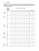
8.0 RAM USAGE The simulation program, to facilitate full usage of the RAM, has organized it into a nominal block of 64 registers, each containing 16 main memory locations and four status locations. Directives which reference RAM as such (i.e., 0, M, and 0), always address it by a register number, and sometimes by a character position within the register. The following chart illustrates this addressing scheme: DIGIT (selected by odd index in SRC instr.) REGISTER (selected by even index in SRC instr.
The bank number in the chart above is the value of the accumulator during a DCl instruction, needed to address that bank of RAMs. The port number given corresponds to the number typed out during simulation of the WMP instruction. Register positions 16-19 (Le., the status locations) are normally addressed in the program by the RDO/WRO, RD 1/WR 1, etc., instructions, respectively.
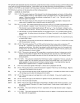
ASTERISK IS SIMULATOR OUTPUT INITIALIZE ~ ~EADY INDICATION MEMORY BLOCK IS ASSIGNED /r .L. *Q0 ., 12!j .10 0:BPP~PNPPPF 01 BPPPPPPPNF 518P.'J:-JPNPPPF 4:8."POl~PPPPF INPUT COMMAND 2:BPP~P~PPNF 618PPNPNPPNF 31BNNNPNPNPF 71BNNNPNPNPF 1 ~::~~~~~~::~: 1 ~:::~:~:~::~ ::~~;~::;:.
FIRST LINE £ *Z *00 2 11 0 0 0 0 0 0 0 20 8 1 0 0 0 0 0 0 0 5 0 0 0 0 1 0 0 " " ., ''"" " " '" " .," "" " "" '" '" ., "" " 0 0 0 0 2 6 0 0 0 11) 0 0 0 0 9 14 10 11 8 11 2 14 0 0 0 0 0 0 0 0 11) 0 0 0 0 0 0 0 0 0 0 0 0 0 0 0 0 0 0 0 0 0 0 0 0 0 4 11 15 1 11 2 15 1 15 6 11 0 0 Ii! 0 0 0 "" *1'118 LOCATION 3 1110 1010 = RDR 0 1 0 " " 0 0 0 0 0 ., .
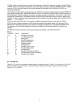
9 14 10 2 I BPPNPNPPNF 61 BPPNPNPPNF 10 I BPPPPPPPPF 141BPPPPPPPPF 01BPPNPNPPPF 41BNPNNPPPPF 81BNPNNPPPPF 121BPPPPPPPPF Figure 9.3 Miscellaneous Directives.
fiH/ 0:START. rIM 4P 0 2: SRC 4P 3: RDR 4ft: XCH 0 5% INC 8 6: SRC 4P 7: RDR 8: XCH I 9: JMS AND II: XCH 2 12: WMP 13: JUN START IS: NOP 16: =104ft 104:/ 104: AND. Cl.B 105: XCH 2 106: l.DM 4 107: XCH 0 108: RAR 109: XCH 0 110: JCN CZ ROTRI 112: XCH I 113: RAR 114: XCH I liS: ROTR2.