IP-4GVI63 Series (Industrial Board) INSTALLATION GUIDE Installation Guide Revision A2 6007002463A20
COPYRIGHT© All rights reserved. The information contained in this guide has been validated and reviewed for accuracy. No patent liability is assumed with respect to the use of the information contained herein. While every precaution has been taken in the preparation of this guide, the Manufacturer assumes no responsibility for errors or omissions.
CONTENTS SECTION 1 INTRODUCTION 1.1 Unpacking IP-4GVI63 Series 1.2 Description 1.3 Features 1.3.1 Graphic & Ethernet 1.3.2 Ultra ATA/66/100 1.3.3 Hardware Monitoring 1.3.4 I/O Shield Connector 1.3.5 Power-On/Off 1.3.6 IP-4GVI63 Series Overview 1.3.7 System Block Diagram 1.4 Specifications 1 1 3 3 3 4 4 4 5 5 6 7 SECTION 2 INSTALLATIONS 2.1 System Installation 2.1.1 CPU Installation 2.1.2 Heat Sink Installation 2.1.3 Memory Module Installation 2.1.4 Setting Jumpers 2.2 Board Layout 2.3 Jumper Setting 2.
CONTENTS SECTION 3 AWARD BIOS SETUP 3.1 BIOS Instructions 3.2 Main Menu 3.3 Standard CMOS Features 3.4 IDE Adapters 3.5 Advanced BIOS Features 3.6 Advanced Chipset Features 3.7 Integrated Peripherals 3.8 Power Management Setup 3.9 PnP/PCI Configurations 3.10 PC Health Status 3.11 Frequency/Voltage Control 3.12 Load Fail-Safe Default 3.13 Load Optimized Defaults 3.14 Supervisor/User Password Setting 3.
iv
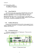
SECTION 1 INTRODUCTION 1.1 Unpacking IP-4GVI63 Series 1. Take out the IP-4GVI63 series unit from the carton box, check if the unit is properly secure in the plastic bag. 2.
Introduction ¡ COM3 ribbon cable (1 Set) (for RS-232/422/485) ¡ I/O Shield 3. Optional Cable ¡ USB2.
Introduction 1.2 Description The IP-4GVI63 Series combines the high performance and exceptional value of Intel® 845GV chipset with a full-featured, new generation, industrial board. The Intel® advanced 845GV chipset support regular socket 478-pins Intel® Pentium® 4 / Celeron® processors of 1.3GHz and up to 3.06GHz, Furthermore, user can set the jumper to select the mobile CPU, that memory base on the FSB 400/533MHz operation supports DDR SDRAM interface.
Introduction ¡ IO Connectivity - ICH4: - 6 Hi-Speed USB2.0 ports - 10/100 Base-TX Ethernet 1.3.2 Ultra ATA/66/100 The ICH4 provides two channel Ultra ATA/66/100 Bus Master IDE controller, that support Ultra ATA/66/100 protocols, perfect for such demanding applications as real-time video, multimedia, and high performance operating system. A new IDE cable is required for Ultra ATA/66/100. This cable is an 80-conductor cable; however the connectors are, of course, backwards compatible with ATA/33. 1.3.
Introduction 1.3.5 Power-On/Off (Remote) The board has a single 20-pins connector for ATX power supplies. For ATX power supplies that support the Remote On/Off feature, this should be connected to the systems front panel for system Power On/Off button. The systems power On/Off button should be a momentary button that is normally open. The board has been designed with “Soft Off" functions.
Introduction System Block Diagram P4 Socket 478-pins VRM ADDR AGP4X DATA GMCH (845GV) 760 FC-BGA CRT Device IDE Primary CTRL Clock DDR266/333 X2 Intel 82562 10/100 Base-TX ATA100 IDE Secondary AC97 Audio Codec ICH4 421 BGA USB Port 1/2 USB PCI SLOTS 1.3.
Introduction 1.4 Specifications ¡ Processor: - Intel® Pentium® 4/Celeron™ processor with socket 478-pins package, Processor operating at 1.3GHz and up to 3.06GHz - Intel® Pentium® 4 Mobile™ processor with socket 478-pins package, Processor operating at 1.2GHz and up to 2.4GHz - System bus frequency at 400/533 MHz FSB ¡ Chipset: - Intel® 82845GV + ICH4 AGPset ¡ DRAM Module: - Two 184-pins Socket - For DDR 266/333 SDRAM memory - Support DDR SDRAM up to 2GB (Max.
Introduction ¡ Onboard PCI / IDE: - Intel® 82801DB (ICH4) controller - PCI rev2.2 Compliant - ACPI Compliant Power Management - PCI bus IDE port with PIO /Ultra DMA-100 x 2 (up to 4 devices) ¡ Rear I/O Connectors: - PS/2 mouse and PS/2 style keyboard - D-Sub 25-pins printer port connector D-Sub 9-pins COM1 serial port connector for RS-232 D-Sub 15-pins VGA connector - 2 x USB2.0 connectors - RJ-45 Ethernet and 2 x USB2.
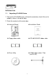
SECTION 2 INSTALLATIONS 2.1 System Installation 2.1.1 CPU Installation Carefully follow the steps below in order to install the CPU: 1. Check and confirm that you are going to install correctly CPU type and pin numbers (figure 3). 2. Lift the releasing lever of the Socket 478. 3. Align the pin of the CPU against the pinholes of the Socket 478. Be sure to pay attention to the orientation of the CPU. Figure 3: CPU Socket 4. Push down the CPU into the Socket 478. 5.
Installations Removing a CPU: 1. Before removing the CPU, turn off the IP-4GVI63 Series power; then wait for about 20 minutes until the heat radiation plate of the cooling fan and the CPU cools down. 2. To remove the CPU, lift the releasing lever of the Socket 478. Note: The CPU and the heat radiation plate are hot. They may cause burns. To remove the CPU, reverse the installation steps. 2.1.
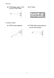
Installations 2.1.3 Memory Module Installation Figure 5 display the notch marks and what they should look like on your DIMM memory module. DIMMs have184-pins and two notches, that will match with the onboard DIMM socket. DIMM modules are installed by placing the chip firmly into the socket at a 90-degree angle and pressing straight down (figure 6) until it fits tightly into the DIMM socket.
Installations Carefully follow the steps below in order to install the DIMMs: 1. To avoid generating static electricity and damaging the DIMM, ground yourself by touching a grounded metal surface or using a ground scrap before you touch the DIMM. 2. Do not touch the connector of the DIMM. Dirt residue may cause a malfunction. 3. Hold the DIMM with its notch to the front side of the IP-4GVI63 Series and insert it completely into the socket. A DIMM should be inserted into the inner socket first.
Installations 2.1.4 Setting Jumpers There are jumpers on the system board of the IP-4GVI63 Series. You can set the jumpers to make the necessary operations. Figure 7: Jumper Connector For any three-pins jumpers (figure 7), the jumper setting is 1-2 when the jumper connects pin 1 and 2. The setting is 2-3 when pin 2 and 3 are connected and so on. You could see one of the lines surrounding jumpers is thick, which indicates pin NO.1.
Installations Board Layout Jumper & Connector Location KBMS1 JP1 FAN2 POWER FAN ATX1 FAN1 LPT1 DIMM2 DIMM1 COM1 CPU FAN VGA1 ATX2 IP-4GVI63 USB1 USB2 LAN CN1 J1 AGP1 CD IN1 AUX IN1 PCI1 ADD ONLY WOL1 PCI2 BAT1 PCI3 PCI4 JBAT1 IDE1 IDE2 COM2 PCI5 JCN1 JPB1 J3 JCN2 JPB2 USB3 FAN4 14 J2 FAN3 FDD1 PCI6 CHASSIS FAN JP3 REV:1.0 2.
Installations 2.3 Jumper Setting Table for Jumper Location Description: Use the information in the following table to change the jumpers.
Installations In order to set up the correct configuration, here is the description about how to set the jumpers to enable/disable or change functions. All jumpers’ location please refer to jumper location diagram.
Installations COM3 port setting select: JPB1 Function RS-232 (Default) RS-422 RS-485 JPB1 1-2 Off On (Term.) On On (Term.) On 3-4 Off (Term.) (Term.) 5-6 Off Off On 7-8 Off On Off 9-10 Off On On 11-12 On Off Off 7-8 Off On Off 9-10 Off On On 11-12 On Off Off y Location: COM4 port setting select: JPB2 Function RS-232 (Default) RS-422 RS-485 JPB2 1-2 Off On (Term.) On On (Term.) On 3-4 Off (Term.) (Term.
Installations Connector’s Description Connector Location KBMS1 JP1 FAN2 POWER FAN ATX1 FAN1 LPT1 DIMM2 DIMM1 COM1 CPU FAN VGA1 ATX2 IP-4GVI63 USB1 USB2 LAN CN1 J1 AGP1 CD IN1 AUX IN1 PCI1 ADD ONLY WOL1 PCI2 BAT1 PCI3 PCI4 JBAT1 IDE1 IDE2 COM2 PCI5 JCN1 JPB1 J3 JCN2 JPB2 USB3 FAN4 18 J2 FAN3 FDD1 PCI6 CHASSIS FAN JP3 REV:1.0 2.
Installations Table for Connector’s Location Description: Use the information in the following table to change the connector.
Installations Primary IDE connector (40-pins 2.
Installations Secondary IDE connector (40-pins 2.
Installations Floppy disk connector (34-pins 2.
Installations PS/2 keyboard connector (6-pins purple Mini Din): KBMS1 Pin # Assignment Pin # Assignment 1 3 5 Keyboard data Ground Keyboard clock 2 4 6 NC +5V NC y Figure: 6 5 4 3 2 1 PS/2 mouse connector (6-pins green Mini Din): KBMS1 Pin # Assignment Pin # Assignment 1 3 5 Mouse data Ground Mouse clock 2 4 6 NC +5V NC y Figure: 6 5 4 3 2 23 1
Installations COM1 RS-232 serial port connector (D-Sub 9-pins male): COM1 Pin # Assignment Pin # Assignment 1 2 3 4 5 DCD (Data Carrier Detect) RXD (Receive Data) TXD (Transmit Data) DTR (Data Terminal Ready) Ground 6 7 8 9 DSR (Data Set Ready) RTS (Request to Send) CTS (Clear to Send) RI (Ring Indicator) y Figure: 1 5 6 9 Parallel port connector (D-Sub 25-pins female): LPT1 Pin # Assignment Pin # Assignment 1 2 3 4 5 6 7 8 9 10 11 12 13 Line Printer Strobe PD 0, Parallel Data 0 PD 1, Parallel
Installations CRT VGA port connector (D-SUB 15-pins female): VGA1 Pin # Assignment Pin # Assignment 1 3 5 7 9 11 13 15 Red Blue Ground Ground VCC NC HSync DDClk 2 4 6 8 10 12 14 Green NC Ground Ground Ground DDData VSync y Figure: 5 1 15 11 USB 1/2 connectors (4-pins female): USB1 Pin # Assignment Pin # 1a 2a 3a 4a VCC USB1 USB1 + Signal ground Assignment 1b 2b 3b 4b VCC USB2 USB2 + Signal ground y Figure: 25 1 4 1 4
Installations USB 3/4 connectors (4-pins female): USB2 Pin # Assignment Pin # 1a 2a 3a 4a VCC USB3 USB3 + Signal ground Assignment 1b 2b 3b 4b VCC USB4 USB4 + Signal ground y Figure: 1 4 1 4 Ethernet (82562ET) RJ-45 connector (RJ-45 phone–jack): LAN Pin # Assignment Pin # Assignment 1 2 3 4 Transmit output (+) Transmit output (-) Receive input (+) NC 5 6 7 8 y Figure: 26 NC Receive input (-) NC NC
Installations Audio port connector: CN1 Pin # Blue Green Red y Figure: Assignment Line-In Line-Out Mic-In Blue Green Red CD_IN connector: CDIN1 Pin # Assignment 1 2 3 4 CD_IN_Left CD_Ground CD_Ground CD_IN_Right y Figure: 27 4 4 1 1
Installations AUX_IN connector: AUXIN1 Pin # Assignment 1 2 3 4 Left Line_IN Ground Ground Right Line_IN_ y Figure: Wake On LAN connector: WOL1 Pin # 4 4 1 1 Assignment 1 2 3 5VSB Ground Data y Figure: 1 28 3
Installations COM2 RS-232 serial port connector (10-pins pin-header): COM2 Pin # Assignment Pin # Assignment 1 3 5 7 9 DCD (Data Carrier Detect) RXD (Receive Data) TXD (Transmit Data) DTR (Data Terminal Ready) Ground 2 4 6 8 10 DSR (Data Set Ready) RTS (Request to Send) CTS (Clear to Send) RI (Ring Indicator) Ground y Figure: 2 10 1 9 COM3 RS-232/422/485 serial port connector (14-pins pin-header): JCN1 Pin # Assignment Pin # Assignment 1 3 5 7 9 11 13 DCD (Data Carrier Detect) RXD (Receive Da
Installations COM4 RS-232/422/485 serial port connector (14-pins pin-header): JCN2 Pin # Assignment Pin # Assignment 1 3 5 7 9 11 13 DCD (Data Carrier Detect) RXD (Receive Data) TXD (Transmit Data) DTR (Data Terminal Ready) Ground TXD+ (Transmit Data+) RXD+ (Receive Data+) 2 4 6 8 10 12 14 DSR (Data Set Ready) RTS (Request to Send) CTS (Clear to Send) RI (Ring Indicator) Ground TXD- (Transmit Data-) RXD- (Receive Data-) y COM4 Figure: 2 14 1 13 Note: How to connect RS485 device with COM port ribb
Installations USB 5/6 pin-header (9-pins pin-header): USB3 Pin # Assignment Pin # 1 3 5 7 9 VCC USB5 USB5 + Ground --- Assignment 2 4 6 8 10 VCC USB6 USB6 + Ground NC y Figure: Power fan power connector: FAN1 Pin # 1 2 3 y Figure: 10 1 9 Assignment Ground +12V Sense 3 31 2 1
Installations CPU fan power connector: FAN2 Pin # 1 2 3 y Figure: Assignment Ground +12V Sense 1 Chassis fan power connector: FAN3 Pin # 1 2 3 y Figure: 3 Assignment Ground +12V Sense 3 1 Fan power connector: FAN4 Pin # 1 2 3 y Figure: Assignment Ground +12V Sense 3 32 1
Installations ATX 12V power connector: ATX1 Pin # Assignment 1 3 Pin # Assignment 2 4 Ground +12V Ground +12V y Figure: ATX power connector: ATX2 Pin # Assignment 1 2 3 4 5 6 7 8 9 10 +3.3V +3.3V Ground +5V Ground +5V Ground PW-OK 5VSB +12V 3 1 4 2 Pin # Assignment 11 12 13 14 15 16 17 18 19 20 +3.
Installations System panel indicate connector: J1 & J2 Pin # J1 Assignment Pin # PWR ON 1 2 PWRBT5VSB 1 2 TB LED 4 5 3 4 5 PWLEDNC PWLED+ SPEAKER HDLED+5V 7 8 9 10 IR 9 10 11 12 13 Ground KBLOCK PWR LED GND +5V HDD LED 6 7 J2 Assignment KEYLOCK IRTX Ground IRRX CIRRX +5V +5V Ground NC BEEP RESET 12 13 Ground RESET+ y Figure: J2 J1 34
Installations Slim floppy disk connector (26-pins FPC connector): J3 Pin # Assignment Pin # Assignment 1 2 3 4 5 6 7 8 9 10 11 12 13 +5V Index +5V Drive_Select +5V Disk_Change NC Ready HD_Out Motor_On Reserve Direction NC 14 15 16 17 18 19 20 21 22 23 24 25 26 Step Ground Write_Data Ground Write_Gate Ground Track Ground Write_Protect Ground Read_Data Ground Side_One y Figure: 1 35 26
SECTION 3 AWARD BIOS SETUP 3.1 BIOS Instructions Award’s ROM BIOS provides a built-in Setup program, which allows user to modify the basic system configuration and hardware parameters. The modified data will be stored in a battery-backed CMOS, so that data will be retained even when the power is turned off. In general, the information saved in the CMOS RAM will stay unchanged unless there is a configuration change in the system, such as hard drive replacement or a device is added.
Award BIOS Setup 3.2 Main Menu Once you enter the AwardBIOS™ CMOS Setup Utility, the Main Menu will appear on the screen. The Main Menu allows you to select from several setup functions and two exit choices. Use the arrow keys to select among the items and press to accept and enter the sub-menu.
Award BIOS Setup Integrated Peripherals: Use this menu to specify your settings for integrated peripherals. See section 4 for the details. Power Management Setup: Use this menu to specify your settings for power management. See section 5 for the details. PnP / PCI Configuration: This entry appears if your system supports PnP / PCI. See section 6 for the details. PC Health Status: Use this menu to show your system temperature, speed and voltage status.
Award BIOS Setup 3.3 Standard CMOS Features The items in Standard CMOS Setup Menu are divided into 10 categories. Each category includes no, one or more than one setup items. Use the arrow keys to highlight the item and then use the or keys to select the value you want in each item.
Award BIOS Setup IDE Secondary Master: Options are in its sub menu (described in 3.4) Press to enter the sub menu of detailed options. IDE Secondary Master: Options are in its sub menu (described in 3.4) Press to enter the sub menu of detailed options. Drive A/ Drive B: Options None 360K, 5.25 in/1.2M, 5.25 in/720K, 3.5 in/ 1.44M, 3.5 in/2.88M, 3.5 in Select the type of floppy disk drive installed in your system. Video: Options EGA/VGA/CGA 40/CGA 80/MONO Select the default video device.
Award BIOS Setup 3.4 IDE Adapters The IDE adapters control the hard disk drive. Use a separate sub menu to configure each hard disk drive. Phoenix - AwardBIOS CMOS Setup Utility IDE Primary Master IDE HDD Auto-Detection Press Enter Item Help ____________________________ IDE Primary Master Access Mode Auto 2557 MB Auto Menu Level Cylinder Head Precomp Landing Zone Sector 4956 16 0 4955 63 ¾¾ To auto-detect the HDD’s size, head...
Award BIOS Setup The following options are selectable only if the ‘IDE Primary Master’ item is set to “Manual” Cylinder: Options Min = 0, Max = 65535 Set the number of cylinders for this hard disk.
Award BIOS Setup 3.5 Advanced BIOS Features This section allows you to configure your system for basic operation. You have the opportunity to select the system’s default speed, boot-up sequence, keyboard operation, shadowing and security. Phoenix - AwardBIOS CMOS Setup Utility Advanced BIOS Features Virus Warning CPU L1 & L2 Cache Quick Power On Self Test APIC Mode HDD S.M.A.R.T. Capability ¾ Boot Seq.
Award BIOS Setup Quick Power On Self Test: This category speeds up Power On Self Test (POST) after you power up the computer. If it is set to Enable, BIOS will shorten or skip some check items during POST. Enabled---Enable quick POST Disabled--- Normal POST APIC Mode: This item allows you to enable/disable APIC Mode. The choice: Enabled, Disabled. HDD S.M.A.R.T Capability: Enabled SMART hard driver functions for compatible. disabled. The choice: Enabled, Disabled. The default is Boot Seq.
Award BIOS Setup Swap Floppy Drive: If the system has two floppy drives, you can swap the logical drive name assignments. The choice: Enabled, Disabled. Boot Up Floppy Seek: Seeks disk drives during boot up. Disabling speeds boot up. The choice: Enabled, Disabled. Report No FDD For Win 95: Whether report no FDD for Win 95 or not. The choice: Yes, No. Boot Up NumLock Status: Select power on state for NumLock.
Award BIOS Setup Security Option: Select whether the password is required every time the system boots or only when you enter setup. System---The system will not boot and access to Setup will be denied if the correct password is not entered at the prompt. Setup---The system will boot, but access to Setup will be denied if the correct password is not entered at the prompt. Note: To disable security, select PASSWORD SETTING at Main Menu and then you will be asked to enter password.
Award BIOS Setup 3.6 Advanced Chipset Features This section allows you to configure the system based on the specific features of the installed chipset. This chipset manages bus speeds and access to system memory resources, such as DRAM and the external cache. It also coordinates communications between the conventional ISA bus and the PCI bus. It must be stated that these items should never need to be altered.
Award BIOS Setup CAS Latency Time: When synchronous DRAM is installed, the number of clock cycles of CAS latency depends on the DRAM timing. The choice: 1.5, 2, and 2.5. Active To Precharge Delay: Select the operating system that is active to precharge delay. The choice: 5, 6, 7. DRAM RAS# To CAS# Delay: This field let’s you insert a timing delay between the CAS and RAS strobe signals, used when DRAM is written to, read from, or refreshed.
Award BIOS Setup Delayed Transaction: The chipset has an embedded 32-bit posted write buffer to support delay transactions cycles. Select “Enabled” to support compliance with PCI specification version 2.1. The choice: Enabled, Disabled. Command Per Clock: Select this item allows the command per clock for system. The choice: Auto, Enabled, Disabled. Fast CS#: Select this item allows the Fast CS# function. The choice: Auto, Enabled, Disabled.
Award BIOS Setup 3.
Award BIOS Setup IDE Primary/Secondary Master/Slave PIO: The four IDE PIO (Programmed Input/Output) fields let you set a PIO mode (0-4) for each of the four IDE devices that the onboard IDE interface supports. Modes 0 through 4 provide successively increased performance. In Auto mode, the system automatically determines the best mode for each device. The choice: Auto, Mode 0, Mode 1, Mode 2, Mode 3 and Mode 4.
Award BIOS Setup USB Keyboard Support: Select “Enabled” if your system contains a Universal Serial Bus (USB) controller and you have a USB keyboard. The choice: Enabled, Disabled. USB Mouse Support: Select “Enabled” if your system contains a Universal Serial Bus (USB) controller and you have a USB mouse. The choice: Enabled, Disabled. AC97 Audio: This item allows you to auto or disable to support AC97 Audio. The choice: Auto, Disabled.
Award BIOS Setup Hot Key Power ON: You can use this item to select operating Hot Key to Power On system. The choice: Ctrl-F1 Onboard FDC Controller: Select “Enabled” if your system has a floppy disk controller (FDC) installed on the system board and you wish to use it. If you install and-in FDC or the system has no floppy drive, select Disabled in this field. The choice: Enabled, Disabled. Onboard Serial Port 1/Port 2: Select an address and corresponding interrupt for the first and second serial ports.
Award BIOS Setup Parallel Port Mode: Select an operating mode for the onboard parallel (printer) port. Select Normal, Compatible, or SPP unless you are certain your hardware and software both support one of the other available modes. The choice: SPP, EPP, ECP and ECP+EPP. EPP Mode Select: Select EPP port type 1.7 or 1.9. The choice: EPP1.7, 1.9. ECP Mode Use DMA: Select a DMA channel for the parallel port for use during ECP mode. The choice: 3, 1.
Award BIOS Setup 3.8 Power Management Setup The Power Management Setup allows you to configure you system to most effectively save energy while operating in a manner consistent with your own style of computer use.
Award BIOS Setup Min. Power Saving: Minimum power management. Doze Mode = 1 hr. Standby Mode = 1 hr., Suspend Mode = 1 hr., and HDD Power Down = 15 min. Max. Power Saving: Maximum power management -- ONLY AVAILABLE FOR SL CPU’s. Doze Mode = 1 min., Standby Mode = 1 min., Suspend Mode = 1 min., and HDD Power Down = 1 min. User Defined: Allow you to set each mode individually. When not disabled, each of the ranges is from 1 min. to 1 hr. except for HDD Power Down, which ranges from 1 min. to 15 min.
Award BIOS Setup Suspend Mode: When “Enabled” and after the set time of system inactivity. All devices except the CPU will be shut off. The choice: Enabled, Disabled. HDD Power Down: When “Enabled” and after the set time of system inactivity, the hard disk drive will be powered down while all other devices remain active. The choice: Enabled, Disabled. Soft-Off by PWR-BTTN: Pressing the power button for more than 4 seconds forces the system to enter the Soft-Off state when the system has “hung.
Award BIOS Setup Reload Global Timer Events: The events are I/O events whose occurrence can prevent the system from entering a power saving mode or can awaken the system from such a mode. In effect, the system remains alert for anything, which occurs to a device, which is configured as Enabled, even when the system is in a power down mode.
Award BIOS Setup 3.9 PnP/PCI Configurations This section describes configuring the PCI bus system. PCI, or Personal Computer Interconnect, is a system, which allows I/O devices to operate at speeds nearing the speed the CPU itself uses when communicating with its own special components. This section covers some very technical items and it is strongly recommended that only experienced users should make any changes to the default settings.
Award BIOS Setup 3.10 PC Health Status Phoenix - AwardBIOS CMOS Setup Utility PC Health Status CPU Warning Temperature Current CPU Temp. Current System Temp. Current Chassis Fan Speed Current CPU Fan Speed Current Power Fan Speed Current CPUFan4 Speed Vagp (V) Vcore (V) Vdimm (V) +5V +12 V Shutdown Temperature Disabled 40°C / 104°F 24°C / 75°F 3283RPM 5152RPM 4182RPM 0 1.52V 1.71V 2.48V 4.81V 11.
Award BIOS Setup Vagp (V) The voltage level of Power supplied to AGP card. Vcore (V) The voltage level of CPU (Vcore). Vdimm (V) The voltage level of the DRAM. +5V/+12V: Show you the voltage of +5V/+12V. Shutdown Temperature: This item allows you to set up the CPU shutdown Temperature. This item is only effective under Windows® 98 ACPI mode. The choice: Disabled, 60°C / 140°F, 65°C / 149°F, 70°C / 159°F and 75°C / 167°F.
Award BIOS Setup 3.11 Frequency/Voltage Control Phoenix - AwardBIOS CMOS Setup Utility Frequency/Voltage Control CPU Clock Ratio Watch Dog Function CPU FSB / SPEED Memory Frequency Next boot AGP/PCI is AGP / PCI Clock AGP/PCI subtle tuning Clock Generation for EMI 22X Enabled Item Help ____________________________ 100MHz/2.
Award BIOS Setup Clock Generation for EMI: Clock Generation for EMI Enabled Auto Detect PCI Clk Spread Spectrum Modulated Disabled Item Help ____________________________ Menu Level ¾ ↑↓←→Move Enter: Select +/-/PU/PD: Value F10: Save ESC: Exit F1: General Help F5: Previous Values F6: Fail-safe defaults F7: Optimized Defaults Auto Detect PCI Clk: When enabled the mainboard automatically disables the clock source for a PCI slot which does not have a module in it, reducing EMI (ElectroMagnetic Interferen
Award BIOS Setup 3.12 Load Fail-Safe Defaults When you press on this item you get a confirmation dialog box with a message similar to: Load Fail-Safe Defaults (Y/N)? N Pressing ‘Y’ loads the BIOS default values for the most stable, minimal-performance system operations. 3.
Award BIOS Setup 3.14 Supervisor/User Password Setting You can set either supervisor or user password, or both of then. The differences between are: Set Supervisor Password: can enter and change the options of the setup menus. Set User Password: just can only enter but do not have the right to change the options of the setup menus. When you select this function, the following message will appear at the center of the screen to assist you in creating a password.
Award BIOS Setup 3.15 Exit Selecting Save & Exit Setup Pressing on this item asks for confirmation: Save to CMOS and EXIT (Y/N)? Y Pressing “Y” stores the selections made in the menus in CMOS – a special section of memory that stays on after you turn your system off. The next time you boot your computer, the BIOS configures your system according to the Setup selections stored in CMOS. After saving the values the system is restarted again.