
User's Manual

4 316704-001 / Development Kit User’s Manual
Figures
Figure 1. Development Board Block Diagram.......................................................24
Figure 2. Development Board Component Locations ............................................. 39
Figure 3. Back Panel Connector Locations ...........................................................42
Figure 4. D-Connector to Component Video Cable................................................43
Figure 5. D-Connector to Composite Video Cable .................................................43
Figure 6. D-Connector to S-Video Cable ............................................................. 43
Figure 7. Configuration Jumper and Switch Locations ...........................................44
Figure 8. LED Locations ...................................................................................48
Figure 9. Heatsink and Backplate ......................................................................64
Figure 10. Backplate Pins .................................................................................65
Figure 11. Applying the Thermal Grease .............................................................66
Figure 12. Squeezing Activation Arm..................................................................66
Figure 13. Installing the Heatsink ...................................................................... 67
Figure 14. Plugging in the Fan ..........................................................................68
Figure 15. Completed Assembly ........................................................................68
Tables
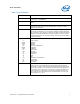
Table 1. Text Conventions ..................................................................................7
Table 2. Terms and Acronyms.............................................................................8
Table 3. Acronyms .........................................................................................10
Table 4. Intel Literature Centers........................................................................ 13
Table 5. Related Documents .............................................................................14
Table 6. Development Board feature Set Summary ..............................................15
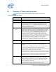
Table 7. BIOS Location Strapping Options........................................................... 30
Table 8. Primary System Clocks ........................................................................31
Table 9. Power Management States ...................................................................32
Table 10. Power Management M-States ..............................................................32
Table 11. Sleep Signals and M-State Definition.................................................... 33
Table 12. Development Board Voltage Rails ........................................................ 34
Table 13. Development Board Component Location Legend ...................................40
Table 14. Back Panel Connector Definitions.........................................................42
Table 15. Supported Configuration Jumper/Switch Settings...................................44
Table 16. LED Functions...................................................................................48
Table 17. Expansion Slots and Sockets...............................................................50
Table 18. PCI Express* (x16) Pinout (J6B2) ........................................................51
Table 19. ADD2 Slot (J6B2).............................................................................. 54
Table 20. MEC Slot (J6B2)................................................................................57
Table 21. PCI Express* (x1) Pinout (J6B1, J7B1, J8B4).........................................60
Table 22. IDE Connector ..................................................................................60
Table 23. SATA Port 0 ‘Direct Connect’ Connector Pinout (J8J1) .............................61
Table 24. SATA Ports 1 and 2 ‘Cable Connect’ Connector Pinout (J7J3, J7H1)...........61
Table 25. SATA Power Connection (J7H2) ...........................................................62
Table 26. Fan Connectors (J2B3, J2C1) ..............................................................62
Table 27. Fan Connector (J2F1) ........................................................................62
Table 28. Front Panel Connector........................................................................62
Table 29. USB Headers ....................................................................................63