LXD9785 PQFP Demo Board with FPGA for SS-SMII (Fiber)-to-MII Conversion Development Kit Manual January 2002 Order Number: 249323-003
Information in this document is provided in connection with Intel® products. No license, express or implied, by estoppel or otherwise, to any intellectual property rights is granted by this document.
Contents Contents 1.0 General Description......................................................................................................................... 7 1.1 2.0 Features................................................................................................................................ 7 Introduction...................................................................................................................................... 9 2.1 2.2 2.3 2.4 Overview.....................
Contents Tables 1 2 3 4 5 6 7 8 9 10 iv Quick-Start Jumper Settings....................................................................................................... 12 Quick-Start Switch Settings ........................................................................................................ 13 Global Configuration Settings (Switch S5) ................................................................................. 14 Global Configuration Settings (Switch S8) ..............................
Contents Revision History Date Revision January 2002 003 March 2001 Page Description All Replaced LXT9785 with LXT9785/9785E globally 16 Added new section 4.5 Expended Temperature Operation with the LXT9785HE. 11 Replaced LXD9785 demo board graphic with A2 version. 12 Quick Start Jumper Settings table: Added JP15 and JP16. 13 Quick Start Switch Settings table: - Removed TxSLEW (S5-1:2) - Renumbered remaining switches - Replaced MDIX with Section and new configuration.
LXD9785 PQFP Demo Board with FPGA for SS-SMII (Fiber)-to-MII Conversion 1.0 General Description The LXD9785 PQFP MII Demo Board is an eight-port 100 Mbps Fast Ethernet Media Access Unit (MAU) that provides a working platform for evaluation of the LXT9785/9785E Fast Ethernet Octal Transceiver. All eight network ports provide a fiber interface for a 100BASE-FX connection.
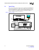
LXD9785 PQFP Demo Board with FPGA for SS-SMII (Fiber)-to-MII Conversion Figure 1.
LXD9785 PQFP Demo Board with FPGA for SS-SMII (Fiber)-to-MII Conversion 2.0 Introduction 2.1 Overview This document describes typical hardware set-up procedures for the LXD9785 PQFP MII Demo Board. To begin immediate operation, a “Quick-Start Checklist” on page 12 supports 100BASEFX operation. Hardware switches and jumpers allow the designer access to all hardware configuration options. Each option is outlined in the “Optional Configurations” on page 14.
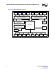
LXD9785 PQFP Demo Board with FPGA for SS-SMII (Fiber)-to-MII Conversion 2.4 Typical Setup Figure 2 shows a typical test setup for standard operation of the LXD9785/9785E PQFP MII Demo Board. The Demo Board plugs into a SmartBits Advanced Multi-port Performance Test Box via eight standard 40-pin MII cables (not included on the board). Eight external NIC cards directly connect to the SmartBits test box and plug into the Demo Board through fiber-module connectors.
LXD9785 PQFP Demo Board with FPGA for SS-SMII (Fiber)-to-MII Conversion Figure 3. LXD9785/9785E SS-SMII Fiber Demo Board Development Kit Manual Document #: 249323 Revision #: 003 Rev.
LXD9785 PQFP Demo Board with FPGA for SS-SMII (Fiber)-to-MII Conversion 3.0 Quick-Start Checklist Use this quick-start procedure for easy setup of the LXD9785 PQFP MII Demo Board. This procedure sets all ports to the default condition (100 Mbps and full-duplex capabilities). 1. Set the jumpers in accordance with Table 1. 2. Set switches S1, S5, and S8 in accordance with Table 2. 3. Connect the eight Demo Board MII ports to the SmartBits test box via MII connector/cables.
LXD9785 PQFP Demo Board with FPGA for SS-SMII (Fiber)-to-MII Conversion Table 2. Quick-Start Switch Settings Switch / Label Setting Configuration Switch S1 S1-1 / ADD_0 0 S1-2 / ADD_1 0 S1-3 / ADD_2 0 S1-4 / ADD_3 0 S1-5 / ADD_4 0 Sets PHY MDIO base address to 00000. Switch S5 S5-1 / PAUSE 0 Disables Pause function. S5-2 / PWRDWN 0 Disables Power-Down function. S5-3 / MDDIS 0 Enables MDIO channel.
LXD9785 PQFP Demo Board with FPGA for SS-SMII (Fiber)-to-MII Conversion 4.0 Optional Configurations 4.1 Global Operating Configurations Switch S5 and S8 configure operating characteristics on all ports of the LXD9875 Demo Board. Each switch can be set manually by toggling the switch either to 1 or 0. Set switches S5 and S8 to the desired configuration according to Table 3 and Table 4 respectively. Table 3.
LXD9785 PQFP Demo Board with FPGA for SS-SMII (Fiber)-to-MII Conversion Table 5. PHY Address Configuration Settings (Switch S1) Jumper / Label Description S1-1 / ADD_0 Address <4:0> - Sets base address. Each port adds its port number (starting with 0) to this address to determine its PHY address. S1-2 / ADD_1 S1-3 / ADD_2 S1-4 / ADD_3 Switch “0” sets address bit to 0. Switch “1” sets address bit to 10.
LXD9785 PQFP Demo Board with FPGA for SS-SMII (Fiber)-to-MII Conversion 4.4 JTAG Test Signals The boundary scan test port is accessed via JP3 for board- level testing. The JTAG test signal descriptions are shown in Table 7. The BSDL file for the LXT9785/9785E is available on the Intel web site at http://developer.intel.com/design/network/. Table 7. JTAG Test Signal Descriptions Jumper Pin# Symbol Description 1 TRST# Test Reset. Input sourced by ATE 3 TCK Test Clock. Input sourced by ATE.
LXD9785 PQFP Demo Board with FPGA for SS-SMII (Fiber)-to-MII Conversion 5.0 LEDs 5.1 Direct Drive LEDs The LXD9785 PQFP MII Demo Board provides three programmable LED drivers per port (D4 D28). Each LED can display one of several available status conditions as selected by the LED Configuration Register (Address 20) shown in Table 8. . Table 8. Direct Drive LED Configuration Settings (Register 20) LED Bits LED1 15:12 LED2 11:8 LED3 Program Bits Description 0000 Indicates 100 Mbps operation.
LXD9785 PQFP Demo Board with FPGA for SS-SMII (Fiber)-to-MII Conversion Table 9. LED Pulse Stretch Settings (Register 20) Bit Name Description Type Default R/W 00 R/W 1 00 = Stretch LED events to 30 ms. 20.3:2 LEDFREQ 01 = Stretch LED events to 60 ms. 10 = Stretch LED events to 100 ms. 11 = Reserved. 20.1 5.2 PULSE- 0 = Disable pulse stretching of all LEDs. STRETCH 1 = Enable pulse stretching of all LEDs.
LXD9785 PQFP Demo Board with FPGA for SS-SMII (Fiber)-to-MII Conversion Board Schematics 6.0 Figure 4. LXD9785 PQFP MII Demo Board Power (Fiber Board Revision A2) VCC $ VCCIO %1 %$1$1$ 2.
1 2 3 4 SECTION RJ11 1 2 3 4 5 6 J3 RJ11 3 2 3 2 TX_CLK0 TX_SYNC0 TX_CLK1 TX_SYNC1 13,16 TX_CLK1 13,16 TX_SYNC1 4.7K GND 3 1 8 7 6 5 8 6 100 B 10 C1 1 LED R611 13 R25 74HC14 U2F GND D156 220 220 D155 VCCIO 74HC14 2 VCCIO U2A LED R610 R15 R16 R17 R10 12 1X8 MODE 220 220 4 TP5 MDINT R12 R13 74HC14 2X4 MODE 3 U2B D93 LED RD D1 LED RD 4.7K 4.7K 4.7K 4.7K 4.7K 4.
1 2 3 4 MDIO0_1 GND GND MDC0_1 3 A 21 22 23 24 25 26 27 28 29 30 31 32 33 34 35 36 37 38 39 40 21 22 23 24 25 26 27 28 29 30 31 32 33 34 35 36 37 38 39 40 MII 40 PIN P2 MII 40 PIN P1 1 2 3 4 5 6 7 8 9 10 11 12 13 14 15 16 17 18 19 20 1 2 3 4 5 6 7 8 9 10 11 12 13 14 15 16 17 18 19 20 R257 R258 R626 R627 R628 R629 R630 R631 50 1% 50 1% 50 1% 50 1% 50 1% 50 1% 50 1% 50 1% ITN_7 IT0_7 IT1_7 IT2_7 IT3_7 50 1% 50 1% 50 1% 50 1% 50 1% TE_7 TN_7 T0_7 T1_7 T2_7 T3_7 ITE_7 50 1% R251 R253 R2
1 2 3 4 GND GND A 21 22 23 24 25 26 27 28 29 30 31 32 33 34 35 36 37 38 39 40 MII 40 PIN MII 40 PIN P4 21 22 23 24 25 26 27 28 29 30 31 32 33 34 35 36 37 38 39 40 P3 1 2 3 4 5 6 7 8 9 10 11 12 13 14 15 16 17 18 19 20 1 2 3 4 5 6 7 8 9 10 11 12 13 14 15 16 17 18 19 20 R283 R284 R592 R593 R594 R595 R596 R597 R303 R305 R306 R307 R308 R301 TE_5 TN_5 T0_5 T1_5 T2_5 T3_5 50 1% 50 1% 50 1% 50 1% 50 1% 50 1% R632 R633 R634 R635 R636 R637 R309 R310 ITE_5 50 1% 50 1% 50 1% 50 1% 50 1% 50 1% IT
1 2 3 4 GND GND MDIO1_1 3 21 22 23 24 25 26 27 28 29 30 31 32 33 34 35 36 37 38 39 40 21 22 23 24 25 26 27 28 29 30 31 32 33 34 35 36 37 38 39 40 MDC1_1 3 A MII 40 PIN P6 MII 40 PIN P5 1 2 3 4 5 6 7 8 9 10 11 12 13 14 15 16 17 18 19 20 1 2 3 4 5 6 7 8 9 10 11 12 13 14 15 16 17 18 19 20 TE_3 TN_3 T0_3 T1_3 T2_3 T3_3 R638 R639 R640 R641 R642 R643 50 1% 50 1% 50 1% 50 1% 50 1% 50 1% ITN_3 IT0_3 IT1_3 IT2_3 IT3_3 50 1% 50 1% 50 1% 50 1% 50 1% 50 1% 50 1% R361 R362 ITE_3 50 1% R355 R357
1 2 3 4 GND GND A 21 22 23 24 25 26 27 28 29 30 31 32 33 34 35 36 37 38 39 40 21 22 23 24 25 26 27 28 29 30 31 32 33 34 35 36 37 38 39 40 MII 40 PIN P8 MII 40 PIN P7 1 2 3 4 5 6 7 8 9 10 11 12 13 14 15 16 17 18 19 20 1 2 3 4 5 6 7 8 9 10 11 12 13 14 15 16 17 18 19 20 R644 R645 R646 R647 R648 R649 18 16 14 12 3 5 7 9 B 1 19 2 4 6 8 17 15 13 11 1G 2G 1A1 1A2 1A3 1A4 2A4 2A3 2A2 2A1 1 19 2 4 6 8 17 15 13 11 GND 1 19 2 4 6 8 17 15 13 11 GND 1 19 2 4 6 8 17 15 13 11 GND CL_0 CR_0 IT
Document #: 249323 Revision #: 003 Rev. Date: January 24, 2002 1 2 3 SD0 SD1 TPFOP1 TPFON1 4 4 4 4 TPFON0 4 4 TPFOP0 4 A TPFON1 TP199 1 R664 50 1% GND C286 0.1uF GND + C282 10uF TPFOP1 R663 50 1% + C285 R659 0.1uF 27 VCC_FX TP198 1 TPFON1 TPFOP1 SD1 SD0 B RD 5 GND 10 9 8 7 TD TD RX Vcc SD RD RX Gnd HFBR_5903 FIBER PORT N/C TX Gnd TX Vcc 5 1 2 3 4 GND + C287 0.1uF TPFIN1 TPFIP1 GND C + C283 0.1uF + C281 0.
1 2 3 4 TPFON3 TPFOP3 SD3 SD2 TPFON2 TPFOP2 A TPFON3 TPFOP3 SD3 SD2 TPFON2 TPFOP2 TP207 1 TP206 1 R681 50 1% + C297 R677 0.1uF 27 B TPFON3 TPFOP3 R682 50 1% + GND + GND C298 0.1uF GND + C294 10uF TPFON2 VCC_FX TPFOP2 TP203 1 R673 50 1% C292 0.1uF GND + C288 10uF B TP202 1 R672 50 1% + C291 R668 0.1uF 27 VCC_FX 6 RD 5 GND 10 9 8 7 TD TD RX Vcc SD RD RX Gnd HFBR_5903 FIBER PORT N/C TX Gnd TX Vcc 5 1 2 3 4 GND GND + C289 0.1uF C + C299 0.
Development Kit Manual TPFON4 6 1 2 TPFOP5 TPFON5 6 SD5 63 6 SD4 6 4 TPFOP4 6 A TPFON5 TPFOP5 SD5 SD4 TPFON4 TPFOP4 TPFOP5 TPFON5 R700 50 1% B + GND + GND C310 0.1uF GND + C306 10uF TP215 1 27 R695 TP214 1 R699 50 1% + C309 0.1uF TPFON4 VCC_FX TPFOP4 R691 50 1% C304 B 0.1uF GND + C300 10uF TP211 1 27 R686 TP210 1 R690 50 1% + C303 0.
1 2 3 4 TPFOP7 TPFON7 7 SD7 7 SD6 7 TPFON6 7 7 TPFOP6 7 A TP223 1 TP222 1 TPFON7 R717 50 1% + C321 R713 0.1uF 27 TPFON7 TPFOP7 R718 50 1% B 0.1uF C322 GND + C318 10uF TPFON6 VCC_FX TPFOP6 R709 50 1% + GND + GND C316 B 0.1uF GND + C312 10uF TP219 1 R708 50 1% + C315 R704 0.1uF 27 TP218 1 TPFOP7 SD7 SD6 TPFON6 TPFOP6 VCC_FX 6 RD 5 GND 10 9 8 7 TD TD RX Vcc SD RD RX Gnd HFBR_5903 FIBER PORT N/C TX Gnd TX Vcc 5 1 2 3 4 GND C + C323 0.
Development Kit Manual Document #: 249323 Revision #: 003 Rev. Date: January 24, 2002 1 2 3 4 GND C117 0.1uF C252 0.01uF C224 0.01uF GND C122 0.1uF VCCA VCC C253 0.1uF A C225 0.1uF C123 0.1uF C46 0.1uF A C52 .01uF C57 0.1uF C58 0.1uF C124 0.1uF C227 0.1uF GND C228 0.01uF C229 0.1uF C254 0.01uF C255 0.1uF C256 0.01uF GND VCC_EXT C257 0.1uF CAPS FOR U22 - U29 C226 0.01uF VCC_EXT B B C231 0.1uF C259 0.1uF C126 .01uF GND C44 0.1uF VCCIO C230 0.01uF C258 0.
1 2 3 VCC_EXT RX_SYNC1 3,16 RX_SYNC1 4 CONF_DONE0 A 3 nSTATUS0 EPC1PC8 nCS OE U6 RX_CLK1 3,16 RX_CLK1 R29 1K RX_SYNC 3,16 RX_SYNC R28 1K RX_CLK GND nCASC DCLK C CONF_DONE1 R550 1K DCLK0 6 X35 4 3 R551 1K VCC_EXT 50 1% TX_CLK0 50 1% TX_SYNC0 SYNC_FPGA_O R562 R563 151 GND 2 SS_SMII_TXCLK SS_SMII_TXSYNC 112 147 SYNC_FPGA_OUT 25 26 130 185 nSTATUS1 B CAP PAD EP20K100QC208-1_SS_SMII SS_SMII_RXCLK SS_SMII_RXSYNC nRESET REF_CLK(125 MHz) U30F nCEO MSEL0 MSEL1 nCE
1 2 SMA(5 PIN) GND 7 1 SMA(5 PIN) GND 7 1 OUT VCC 8 14 OUT VCC 8 14 A GND J5 125 MHzCRYSTAL OSC GND NC Y2 GND J4 125 MHzCRYSTAL OSC GND NC Y1 FB8 50 1% R732 VCCX 50 1% R454 VCCX C350 0.1uF C156 0.1uF 1K 1K 1K B 1K R733 R734 R735 R736 VCC_EXT GND C351 0.01uF GND C157 0.
*1' 5 5 5 5 5 5 5 5 5 5 5 5 $ $ /,1. '83/(; 63((' /,1. '83/(; 63((' /,1. '83/(; 63((' /,1.
1 2 3 RXD_P5 RXD_P6 RXD_P7 TXD_P4 TXD_P5 TXD_P6 TXD_P7 7 6 6 7 7 RX_SYNC1 3,13 7 RX_CLK1 3,13 6 TX_SYNC1 3,13 RXD_P4 TX_CLK1 3,13 6 TXD_P3 TX_SYNC0 3,13 TXD_P2 TX_CLK0 3,13 5 RXD_P3 5 5 RXD_P2 5 TXD_P1 RXD_P1 4 4 RXD_P0 4 TXD_P0 RX_SYNC 3,13 4 RX_CLK 3,13 A TXD_P7 TXD_P6 TXD_P5 TXD_P4 RXD_P7 RXD_P6 RXD_P5 RXD_P4 RX_SYNC1 RX_CLK1 TX_SYNC1 TX_CLK1 TXD_P3 TXD_P2 TXD_P1 TXD_P0 TX_SYNC0 TX_CLK0 RXD_P3 RXD_P2 RXD_P1 RXD_P0 RX_SYNC RX_CLK
1 2 3 4 MDC0_FIX MDIO0_FIX 3 A MDIO0_FIX MDC0_FIX MDC0_FIX R727 0 OHMS B 2 MDIO0_FIX 3 1 PLD0_OE1 GND 2 MDIO0 3 1 3 2 1 PLD0_OE0 GND GND B NC7SZ125M5 GND A OE U37 Y VCC Y VCC Y VCC 0 OHMS NC7SZ125M5 GND A OE U35 R737 NC7SZ125M5 GND A OE U34 4 5 4 5 4 5 R582 R575 50 1% GND C267 0.01uF VCC_MDIO 50 1% GND C266 0.01uF VCC_MDIO R574 GND C260 0.
1 2 3 4 MDC1_FIX MDIO1_FIX 3 A MDIO1_FIX MDC1_FIX MDC1_FIX R729 0 OHMS B 2 MDIO1_FIX 3 1 PLD1_OE1 GND 2 MDIO1 3 1 3 2 1 PLD1_OE0 GND GND B NC7SZ125M5 GND A OE U43 Y VCC Y VCC Y VCC 0 OHMS NC7SZ125M5 GND A OE U41 R730 NC7SZ125M5 GND A OE U40 4 5 4 5 4 5 R623 R618 50 1% GND C353 0.01uF VCC_MDIO 50 1% GND C352 0.01uF VCC_MDIO R615 GND C354 0.
LXD9785 PQFP Demo Board with FPGA for SS-SMII (Fiber)-to-MII Conversion 7.0 Bill of Materials Table 10.
LXD9785 PQFP Demo Board with FPGA for SS-SMII (Fiber)-to-MII Conversion Table 10.
LXD9785 PQFP Demo Board with FPGA for SS-SMII (Fiber)-to-MII Conversion Table 10. LXD9785 Bill of Materials (Fiber - SS-SMII) (Continued) Reference Designator 38 Description Manufacturer Part Number R651, 656, 657, 660, 665, 666, 669, 674, 675, 678, 683, 684, 687, 692, 693, 696, 701, 702, 705, 710, 711, 714, 719, 720 RES 130 OHM 1/ 10W 1% (0805) SMD PANASONIC ERJ-6ENF1300V R658, 667, 676, 685, 694, 703, 712, 721 RES 82.
LXD9785 PQFP Demo Board with FPGA for SS-SMII (Fiber)-to-MII Conversion Table 10. LXD9785 Bill of Materials (Fiber - SS-SMII) (Continued) Reference Designator Description Manufacturer (DO NOT INSTALL U34, 35, 37, 40, 41, 43) IC LOGIC NC7SZ125 SINGLE TRISTATE BUFFER SOT23 FAIRCHILD SEMICONDUCTOR NC7SZ125M5 U46 (DO NOT INSTALL U36, 42) IC FPGA 7032A 3.3V PROGRAMMABLE PLD 44 PIN TQFP ALTERA EPM7032AETC44-4 Y1, 2 (DO NOT INSTALL) OSC 125.000MHZ 25PPM 3.