AI5VG Pentium VP3 Baby AT Motherboard User’s Manual Version 2.
Contents Contents Chapter 1 Introduction.................................................... 1 Chapter 2 Specifications .................................................. 2 Chapter 3 Hardware Description ................................... 4 3.1 Processor and CPU Voltage ..............................................6 3.2 L2 Cache Memory .............................................................6 3.3 Main Memory ....................................................................6 3.4 BIOS .............
Contents Chapter 6 BIOS Configuration..................................... 29 6.1 BIOS Introduction ...........................................................32 6.2 BIOS Setup ......................................................................32 6.3 Standard CMOS Setup.....................................................34 6.4 BIOS Features Setup .......................................................37 6.5 Chipset Features Setup ....................................................40 6.
Chapter 1 Introduction Chapter 1 Introduction This manual is designed to give you information on the AI5VG Motherboard. It is divided into the following six sections: • Introduction • Specifications • Hardware Description • Hardware Settings • Installation • BIOS Configuration Checklist Please check that your package is complete and contains the items below. If you discover damaged or missing items, please contact your dealer.
Chapter 2 Specifications Chapter 2 Specifications Based on VIA’s VP3AT chipset, the AI5VG is a Baby AT Pentium motherboard that supports all the features to make a Microsoft PC’97 compliant PCI/ISA system. This high performance model comes with an Accelerated Graphics Port (AGP) slot, power management functionality that is compliant with ACPI (Advanced Configuration and Power Interface) and legacy APM requirements.
Chapter 2 Specifications Onboard Bus Mastering EIDE Two EIDE interfaces for up to four devices, support PIO Mode 3/4 or Ultra DMA/33 IDE Hard Disk and ATAPI CD-ROM. BIOS Licensed BIOS with additional features: • FLASH EEPROM (128KB) for BIOS update • ISA Plug and Play (PnP) extension • Power management CPU Temperature Sensor The AD22105 IC on the motherboard is a temperature sensor for the CPU.
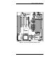
Chapter 3 Hardware Description Chapter 3 Hardware Description This chapter briefly describes each of the major features of the AI5VG motherboard. The layout of the board is shown in Figure 1 which shows the locations of the key components. The topics covered in this chapter are as follows: 3.1 Processor and CPU Voltage.......................................................6 3.2 L2 Cache Memory .....................................................................6 3.3 Main Memory ...........................
Chapter 3 Hardware Description Figure 1: Layout of the AI5VG Motherboard AI5VG Pentium VP3 Baby AT Motherboard User’s Manual 5
Chapter 3 Hardware Description 3.1 Processor and CPU Voltage The AI5VG is designed to take a Pentium Processor with a bus speed of 60 and 66 MHz. The internal clock of the CPU can be multiples of 1.5, 2, 2.5, 3, 3.5, 4 and 4.5 of the bus clock, the CPU frequency can be 90 to 300MHz. The onboard CPU voltage regulator provides support for CPUs Vcore which require voltage other than 3.3V such as 2.8V, and/or power consumption higher than 10 watts. 3.2 L2 Cache Memory The AI5VG supports 512KB P.B.
Chapter 3 Hardware Description (1) 72-pin SIMM (5V) EDO DRAM Bank0 Bank1 Total Memory (SIMM1, SIMM2) (SIMM3, SIMM4) ----8MB 4MB×2 ----16MB 8MB×2 ----32MB 16MB×2 ----64MB 32MB×2 ----128MB 64MB×2 16MB 4MB×2 4MB×2 24MB 8MB×2 4MB×2 40MB 16MB×2 4MB×2 72MB 32MB×2 4MB×2 136MB 64MB×2 4MB×2 32MB 8MB×2 8MB×2 48MB 16MB×2 8MB×2 80MB 32MB×2 8MB×2 144MB 64MB×2 8MB×2 64MB 16MB×2 16MB×2 96MB 32MB×2 16MB×2 160MB 64MB×2 16MB×2 128MB 32MB×2 32MB×2 192MB 64MB×2 32MB×2 256MB 64MB×2 64MB×2 AI5VG Pentium VP3 Baby AT Motherboard
Chapter 3 Hardware Description (2) 168-pin DIMM (3.3V) SDRAM or EDO DRAM Bank0 (DIMM2) Bank1 (DIMM1) Total Memory 8MB ----8MB 16MB ----16MB 32MB ----32MB 64MB ----64MB 128MB ----128MB 8MB 8MB 16MB 16MB 8MB 24MB 32MB 8MB 40MB 64MB 8MB 72MB 128MB 8MB 136MB 16MB 16MB 32MB 32MB 16MB 48MB 64MB 16MB 80MB 128MB 16MB 144MB 32MB 32MB 64MB 64MB 32MB 96MB 128MB 32MB 160MB 64MB 64MB 128MB 128MB 64MB 192MB 128MB 128MB 256MB 3.
Chapter 3 Hardware Description 3. Power Management The power management feature provides power savings by slowing down the CPU clock, turning off the monitor screen and stopping the HDD spindle motor. 3.5 Onboard PCI EIDE The PCI EIDE controller is part of the VP3AT chipset. It supports PIO mode 3/4 and bus mastering . The peak transfer rate of PIO mode 3/4 can be as high as 17MB/sec. Using HDDs that support bus mastering, the peak transfer rate can reach 22MB/sec.
Chapter 3 Hardware Description 3.8 I/O Port Address Map Each peripheral device in the system is assigned a set of I/O port addresses which also becomes the identity of the device. There are a total of 1K port address space available. The following table lists the I/O port addresses used on the motherboard.
Chapter 3 Hardware Description 3.10 Interrupt Request Lines (IRQ) There are a total of 15 IRQ lines available on the motherboard. Peripheral devices use interrupt request lines to notify the CPU for the service required. The following table shows the IRQ used by the devices on the motherboard.
Chapter 4 Hardware Settings Chapter 4 Hardware Settings The following sections describe the necessary procedures and proper jumper settings to configure the AI5VG motherboard. 4.1 SW1(1-8): CPU Frequency Selector .........................................14 4.2 SW2(1-4): CPU Voltage Selector .............................................16 4.3 JP5: Clear CMOS Selection ......................................................18 For the locations of the jumpers, refer to Figure 2 on the following page.
Chapter 4 Hardware Settings Figure 2: Jumper Locations of the AI5VG AI5VG Pentium VP3 Baby AT Motherboard User’s Manual 13
Chapter 4 Hardware Settings 4.1 SW1(1-8): CPU Frequency Selector For Intel Pentium CPU SW1 Bus Clock Mutiplier CPU FREQ. 60MHz 1.5x P54C-90 66MHz 1.5x P54C-100 60MHz 2x P54C-120 66MHz 2x P54C-133 60MHz 2.5x P54C-150 66MHz 2.5x P54C/P55C-16 6 66MHz 3x P54C/P55C-20 0 66MHz 3.
Chapter 4 Hardware Settings For Cyrix 6x86, 6x86L CPU SW1 Bus Clock Mutiplier CPU FREQ. 60MHz 2x P150+ (120MHz) 66MHz 2x P166+ (133MHz) on off off off on off off off off off off off on off off off For Cyrix 6x86MX CPU SW1 Bus Clock Mutiplier CPU FREQ. 66MHz 2.5x PR200 (166MHz) 66MHz 3x PR233 (200MHz) 66MHz 3.5x PR266 (233MHz) off off off off on on off off off off off off off on off off off off off off off off For AMD K5, K6 CPU SW1 Bus Clock Mutiplier CPU FREQ. 60MHz 1.
Chapter 4 Hardware Settings SW1 Bus Clock Mutiplier CPU FREQ. 66MHz 2.5x PR166 / K6-166 66MHz 3x K6-200 66MHz 3.5x K6-233 off off off off on on off off off off off off off on off off off off off off off off off off 4.2 SW2(1-4): CPU Voltage Selector For Single Voltage CPU: Intel P54C, Cyrix 6x86, AMD K5, C6 SW2 VIO VCORE 3.5V 3.5V on on on on For Dual Voltage CPU: Intel P55C, Cyrix 6x86L/MX, AMD K6 SW2 VIO VCORE 3.3V 3.5V 3.3V 3.4V 3.3V 3.
Chapter 4 Hardware Settings For Dual Voltage CPU: Intel P55C, Cyrix 6x86L/MX, AMD K6 SW2 VIO VCORE CPU 3.3V 3.2V K6-233 (0.35µ) 3.3V 3.1V 3.3V 3.0V 3.3V 2.9V K6-166/200 6x86MX 3.3V 2.8V P55C 6x86L 3.3V 2.7V 3.3V 2.6V 3.3V 2.5V 3.3V 2.4V 3.3V 2.
Chapter 4 Hardware Settings For Dual Voltage CPU: Intel P55C, Cyrix 6x86L/MX, AMD K6 SW2 VIO VCORE CPU 3.3V 2.2V K6-233 (0.25µ) 3.3V 2.1V K6-233 (0.25µ) 3.3V 2.0V off on off off on off off off off off off off 4.3 JP5: Clear CMOS Selection Use JP5, a 3-pin header, to clear the contents of the CMOS RAM. Do not clear the CMOS RAM unless it is absolutely necessary. You will lose your password, etc.
Chapter 5 Installation Chapter 5 Installation This chapter describes the connectors and interfaces that the AI5VG provides for creating a working system. Refer to Figure 3 for the location of the connectors. The following items are covered in this chapter: 5.1 I/O Connectors .......................................................................... 21 5.2 J3: AT Power Supply Connector............................................... 21 5.3 J2: ATX Power Supply Connector.......................................
Chapter 5 Installation Figure 3: Connector Location on the AI5VG 20 AI5VG Pentium VP3 Baby AT Motherboard User’s Manual
Chapter 5 Installation 5.1 I/O Connectors The I/O connectors connect the AI5VG to the most common peripherals. To attach cables to these connectors, carefully align Pin 1 of the cables to that of the connectors. Refer to Figure 4 for the location and orientation of the connectors. Figure 4: Orientation of the I/O Connector 5.2 J3: AT Power Supply Connector When using an AT compatible power supply, plug both of the power supply connectors into J3.
Chapter 5 Installation 5.3 J2: ATX Power Supply Connector J2 is a 20-pin ATX power supply connector. Refer to the following table for the pin out assignments. 11 1 20 10 Signal Name 3.3V -12V Ground PS-ON Ground Ground Ground -5V +5V +5V Pin # 11 12 13 14 15 16 17 18 19 20 Pin # 1 2 3 4 5 6 7 8 9 10 Signal Name 3.3V 3.3V Ground +5V Ground +5V Ground Power good 5VSB +12V 5.
Chapter 5 Installation 5.5 J7, J6: Serial Ports The onboard serial ports of the AI5VG are 10 pin-header connectors. J7 is COM1 and J6 is COM2. The following table shows the pin out of the these connectors. Pin # 1 2 3 4 5 6 7 8 9 10 Signal Name DCD, Data carrier detect RXD, Receive data TXD, Transmit data DTR, Data terminal ready GND, ground DSR, Data set ready RTS, Request to send CTS, Clear to send RI, Ring indicator Not Used 5.
Chapter 5 Installation 5.
Chapter 5 Installation 5.8 J10: Parallel Port Connector The following table describes the pin out assignments of this connector.
Chapter 5 Installation 5.11 J13 Wake on LAN Connector J13is a 3-pin header for Wake on LAN function on the motherboard. 1 2 3 Pin # Signal Name 1 2 3 5VSB Ground Wake on LAN 5.12 J14: CPU Fan Power Connector J14 is a 3-pin header for the CPU fan power connector. The fan must be a 12V fan. 1 2 3 Pin # Signal Name 1 2 3 Rotation +12V Ground 5.
Chapter 5 Installation Speaker: Pins 1 - 4 This connector provides an interface to a speaker for audio tone generation. An 8-ohm speaker is recommended. J20 Pin # 1 2 3 4 Signal Name Speaker out No connect Ground +5V Power LED and Keylock: Pins 11 - 15 The power LED indicates the status of the main power switch. The keylock switch, when closed, will disable the keyboard function.
Chapter 5 Installation Reset Switch: Pins 9 and 19 The reset switch allows the user to reset the system without turning the main power switch Off and then On. Orientation is not required when making a connection to this header. Hard Disk Drive LED Connector: Pins 10 and 20 This connector connects to the hard drive activity LED on control panel. This LED will flash when the HDD is being accessed.
Chapter 7 LANDesk User Guide Chapter 6 BIOS Configuration This chapter describes the different settings available in the Award BIOS that comes with the AI5VG motherboard. The topics covered in this chapter are as follows: 6.1 BIOS Introduction..................................................................... 32 6.2 BIOS Setup ............................................................................... 32 6.3 Standard CMOS Setup ..............................................................
Chapter 7 LANDesk User Guide Cache Rd+CPU Wt Pipeline Read Around Write Cache Timing Video BIOS Cacheable System BIOS Cacheable Memory Hole at 15MB Addr. AGP Aperture Size OnChip USB 6.6 Power Management Setup .........................................................42 Power Management PM Control by APM Video Off Method Modem Use IRQ Soft-Off by PWRBTN HDD Power Down Doze Mode Suspend Mode PM Events 6.
Chapter 7 LANDesk User Guide IDE Primary/Secondary Master/Slave PIO IDE Primary/Secondary Master/Slave UDMA Onboard FDD Controller Onboard Serial/Parallel Port UART 2 Mode Onboard Parallel Mode 6.11 Supervisor / User Password..................................................... 51 6.12 IDE HDD Auto Detection ....................................................... 52 6.13 HDD Low Level Format ......................................................... 52 6.14 Save & Exit Setup ................................
Chapter 7 LANDesk User Guide 6.1 BIOS Introduction The Award BIOS (Basic Input/Output System) installed in your computer system’s ROM supports Intel/Cyrix/AMD processors in a standard IBM-AT compatible I/O system. The BIOS provides critical low-level support for standard devices such as disk drives, serial and parallel ports. It also adds virus and password protection as well as special support for detailed fine-tuning of the chipset controlling the entire system. 6.
Chapter 7 LANDesk User Guide ROM PCI/ISA BIOS CMOS SETUP UTILITY AWARD SOFTWARE, INC.
Chapter 7 LANDesk User Guide 6.3 Standard CMOS Setup “Standard CMOS Setup” choice allows you to record some basic hardware configurations in your computer system and set the system clock and error handling. If the motherboard is already installed in a working system, you will not need to select this option. You will need to run the Standard CMOS option, however, if you change your system hardware configurations, the onboard battery fails, or the configuration stored in the CMOS memory was lost or damaged.
Chapter 7 LANDesk User Guide Time The time format is: Hour : 00 to 23 Minute : 00 to 59 Second : 00 to 59 To set the time, highlight the “Time” field and use the / or +/- keys to set the current time. Primary HDDs / Secondary HDDs The onboard PCI IDE connectors provide Primary and Secondary channels for connecting up to four IDE hard disks or other IDE devices. Each channel can support up to two hard disks; the first is the “Master” and the second is the “Slave”.
Chapter 7 LANDesk User Guide NOTE: The specifications of your drive must match with the drive table. The hard disk will not work properly if you enter incorrect information in these fields. If your hard disk drive type is not matched or listed, you can use Type User to define your own drive type manually. Drive A / Drive B These fields identify the types of floppy disk drive A or drive B that has been installed in the computer. The available specifications are: 360KB 1.2MB 720KB 1.44MB 2.88MB 5.25 in. 5.
Chapter 7 LANDesk User Guide 6.4 BIOS Features Setup This section allows you to configure and improve your system and allows you to set up some system features according to your preference. ROM / PCI ISA BIOS BIOS FEATURES SETUP AWARD SOFTWARE, INC.
Chapter 7 LANDesk User Guide Quick Power On Self Test This choice speeds up the Power On Self Test (POST) after you power up the system. If it is set to Enabled, BIOS will skip some items. By default, this choice is Enabled. Boot Sequence This field determines the drive that the system searches first for an operating system. The options are : A, C, SCSI D, A, SCSI SCSI, C, A C, A, SCSI E, A, SCSI C only C, CDROM, A F, A, SCSI LS/ZIP, C CDROM, C, A SCSI, A, C The default value is A, C, SCSI.
Chapter 7 LANDesk User Guide Typematic Rate Setting When disabled, continually holding down a key on your keyboard will generate only one instance. When enabled, you can set the two typematic controls listed next. By default, this field is set to Disabled. Typematic Rate (Chars/Sec) When the typematic rate is enabled, the system registers repeated keystrokes speeds. You can select speed range from 6 to 30 characters per second. By default, this item is set to 6.
Chapter 7 LANDesk User Guide 6.5 Chipset Features Setup This Setup menu controls the configuration of the motherboard chipset. ROM PCI/ISA BIOS CHIPSET FEATURES SETUP AWARD SOFTWARE INC.
Chapter 7 LANDesk User Guide Cache Timing This field sets the timing of the cache in the system. The options are Fast and Fastest. By default, this field is set to Fast. Video BIOS Cacheable When enabled, access to video BIOS addressed at C0000H to C7FFFH are cached, provided that the cache controller is enabled. System BIOS Cacheable When enabled, access to the system BIOS ROM addressed at F0000H-FFFFFH are cached, provided that the cache controller is enabled. Memory Hole at 15MB Addr.
Chapter 7 LANDesk User Guide 6.6 Power Management Setup The Power Management Setup allows you to save energy of your system effectively. It will shut down the hard disk and turn off video display after a period of inactivity. ROM PCI/ISA BIOS (2A59IM29) POWER MANAGEMENT SETUP AWARD SOFTWARE, INC.
Chapter 7 LANDesk User Guide PM Control by APM This field allows you to use the Advanced Power Management device to enhance the Max. Power Saving mode and stop the CPU’s internal clock. If the Max. Power Saving is not enabled, this will be preset to NO. Video Off Method This field defines the Video Off features. There are three options. V/H SYNC + Blank Default setting, blank the screen and turn off vertical and horizontal scanning.
Chapter 7 LANDesk User Guide PM Events The VGA, LPT & COM, HDD & FDD, DMA /master, Modem Ring Resume, RTC Alarm Resume and Primary INTR section are I/O events which can prevent the system from entering a power saving mode or can awaken the system from such a mode. When an I/O device wants to gain the attention of the operating system, it signals this by causing an IRQ to occur. When the operating system is ready to respond to the request, it interrupts itself and performs the service.
Chapter 7 LANDesk User Guide 6.7 PNP/PCI Configuration This option configures the PCI bus system. All PCI bus systems on the system use INT#, thus all installed PCI cards must be set to this value. ROM PCI/ISA BIOS CHIPSET FEATURES SETUP AWARD SOFTWARE INC.
Chapter 7 LANDesk User Guide CPU to PCI Write Buffer When enabled, this option increase the efficiency of the PCI bus to and speed up the execution in the processor. By default, this field is set to Enabled. PCI Dynamic Bursting When enabled, this option combines several PCI cycles into one. By default, this field is set to Disabled. PCI Master 0 WS Write When enabled, this option increases the write cycle speed. By default, this field is set to Disabled.
Chapter 7 LANDesk User Guide PCI IDE IRQ Map To This field allows you to configure the type of IDE disk controller in your system. The default setup is ISA. If you have equipped with PCI controller, you need to specify which slot has the controller and PCI interrupt is associated with the connected hard drives. Selecting “PCI AUTO” allows the system to automatically determine your IDE disk system configuration.
Chapter 7 LANDesk User Guide 6.8 Load BIOS Defaults This option allows you to load the troubleshooting default values permanently stored in the BIOS ROM. These default settings are non-optimal and disable all high-performance features. ROM PCI/ISA BIOS CMOS SETUP UTILITY AWARD SOFTWARE, INC.
Chapter 7 LANDesk User Guide 6.10 Integrated Peripherals This option sets your hard disk configuration, mode and port. ROM PCI/ISA BIOS CHIPSET FEATURES SETUP AWARD SOFTWARE INC.
Chapter 7 LANDesk User Guide The system supports five modes, numbered from 0 (default) to 4, which primarily differ in timing. When Auto is selected, the BIOS will select the best available mode. IDE Primary/Secondary Master/Slave UDMA This field allows your system to improve disk I/O throughput to 33Mb/sec with the Ultra DMA/33 feature. The options are Auto and Disabled. Onboard FDD Controller This option allows you to select the onboard FDD port.
Chapter 7 LANDesk User Guide 6.11 Supervisor / User Password These two options set the system password. Supervisor Password sets a password that will be used to protect the system and Setup utility. User Password sets a password that will be used exclusively on the system. To specify a password, highlight the type you want and press . The Enter Password: message prompts on the screen. Type the password, up to eight characters in length, and press .
Chapter 7 LANDesk User Guide 6.12 IDE HDD Auto Detection This option detects the parameters of an IDE hard disk drive, and automatically enters them into the Standard CMOS Setup screen. ROM PCI/ISA BIOS STANDARD CMOS SETUP AWARD SOFTWARE, INC.
Chapter 7 LANDesk User Guide 6.14 Save & Exit Setup This option allows you to determine whether to accept the modifications or not. If you type “Y”, you will quit the setup utility and save all changes into the CMOS memory. If you type “N”, you will return to Setup utility. ROM PCI/ISA BIOS CMOS SETUP UTILITY AWARD SOFTWARE, INC.