Intel® Embedded Compact Extended Form Factor Proof-of-Concept Board Based on Intel® 915GM Chipset User’s Manual June 2007 Order Number: 310915-002
Contents INFORMATION IN THIS DOCUMENT IS PROVIDED IN CONNECTION WITH INTELR PRODUCTS. EXCEPT AS PROVIDED IN INTEL’S TERMS AND CONDITIONS OF SALE FOR SUCH PRODUCTS, INTEL ASSUMES NO LIABILITY WHATSOEVER, AND INTEL DISCLAIMS ANY EXPRESS OR IMPLIED WARRANTY RELATING TO SALE AND/OR USE OF INTEL PRODUCTS, INCLUDING LIABILITY OR WARRANTIES RELATING TO FITNESS FOR A PARTICULAR PURPOSE, MERCHANTABILITY, OR INFRINGEMENT OF ANY PATENT, COPYRIGHT, OR OTHER INTELLECTUAL PROPERTY RIGHT.
Contents Contents 1 Product Overview ............................................................................................................5 1.1 Introduction ...........................................................................................................5 1.2 Related Documents...............................................................................................5 1.3 Product Contents ..................................................................................................
Contents Table 18. LVDS Connector (CN6)....................................................................................19 Table 19. Power Connector (CN7) ...................................................................................19 Table 20. LVDS Voltage Connector (CN8) .......................................................................19 Table 21. Serial Port2 Connector (CN9)...........................................................................20 Table 22. LAN Connector (CN10) .......
Product Overview 1 1.1 Product Overview Introduction The Proof of Concept board utilizes the Intel® Pentium® M Processor Low Voltage 738 or Intel® Celeron® M Processor Ultra Low Voltage 373, and the Intel® 915GM and Intel® I/O Controller Hub 6-M (ICH6-M) chipset. It is a fanless design which provides higher processing capability with excellent power consumption control. It offers a stable and efficient solution for customer who is seeking a trade-off between high performance and low power consumption.
Product Overview 1.3 Product Contents The Intel® ECX Form Factor POC board based on Intel® 915GM chipset is shipped with the following peripherals: 1.
Product Overview Display: y Analog CRT DAC interface support - 24-bit RAMDAC support (8-bit for each RGB signal DAC) - Resolution up to 2048 x 1536 at 75Hz - DDC2B compliant y Analog TV-Out interface support - On board S-Video 4-pin mini DIN connector y Dedicated Local Flat Panel(LFP) LVDS interface - Compliant with ANSI/TIA/EIA-644-2001 spec - Supports 25 to 112 MHz single/dual channel LVDS interface with Spread Spectrum Clocking (SSC) - Support TFT panel type with maximum pixel format of 1x18 bpp for sin
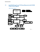
Product Overview 1.5 Intel® ECX Form Factor POC Board Based on Intel® 915GM Chipset Block Diagram Figure 1. Block Diagram Intel® Pentium® M LV 738 or Intel® Celeron® M ULV 373 Processor CK-410 DC/DC IMVP IV CK-SSCD DC-DC GMCH, DDR2 479 uPCBCA FSB 400 LVDS Intel® 915GM GMCH VGA DDR2 SO-DIMM DDR2 400 SDV0 TVOUT 1257 FCBCA DMI SATA x 1 Intel® 82801FBM ICH6-M PATA, CF USB 2.
Installation Guide for POC Board 2 2.1 Installation Guide for POC Board Before You Begin Table 2 shows the additional hardware that may be needed to set up the board. Table 2. Additional Hardware Component 2.2 Description VGA Monitor Standard VGA or greater resolution monitor. Keyboard Keyboard with a PS/2 connector or adapter. Mouse Mouse with a PS/2 connector or adapter. IDE Devices Up to two IDE devices can be connected to the POC board. One cable is included in this kit.
Installation Guide for POC Board 2. Verify contents. Inspect the contents of your kit, and ensure that everything listed in Section 1.3 is included. Check for damage that may have occurred during shipment. 3. Check jumper settings. Verify that the following jumpers are set in their default state (see Table 3). Table 3.
Installation Guide for POC Board Figure 2. Assembly board, Top View Figure 3.
Installation Guide for POC Board 6. Install storage devices. There is one IDE and one SATA connector on the POC board, which supports up to 3 hard drives (two PATA IDE devices—a master and a slave and one SATA IDE device. Note: Master/slave settings are determined by a jumper on each IDE device. Consult the device label/documentation to verify that the jumper is set correctly for the configuration you choose. A CD-ROM drive or additional hard drive may be installed as a primary slave device.
Installation Guide for POC Board Notes: Powering up without all components installed correctly could lead to a power-up failure that could damage that board. Do not power up the board until the source of any loose components is fixed and the component has been replaced on the board.
Connectors and Jumpers 3 Connectors and Jumpers This section describes the placement of the connectors as well as jumper settings on the board. Figure 5.
Connectors and Jumpers Figure 6. Solder Side 3.1 List of Jumpers Table 4 to Table 9 must be used in setting the jumpers on the POC board. These tables give details about the jumpers shown in Figure 5 and Figure 6. The jumpers allow configuring the system to user’s application. The table below shows the function of each of the board’s jumpers: Table 4.
Connectors and Jumpers Table 5. Compact Flash Power Select (JP1) Option 3.3 V (default) 5V JP1 Short 1-2 Short 2-3 Table 6. LVDS Voltage select (JP2) Option 3.3 V (default) 5V JP2 Short 1-2 Short 2-3 Table 7. COM1 Mode Select for RS-232/422/485 (JP3/JP6/JP7) Option RS232 (default) RS422 RS485 JP3 Short 3-5, 4-6 Short 1-3, 2-4 Short 1-3, 2-4 Table 8. COM1 Mode Select (JP4) Option Pin 1=DCD (default) Pin 1=5 V Pin 8=RI (default) Pin 8=+12 V JP4 Short 3-5 Short 1-3 Short 4-6 Short 2-4 Table 9.
Connectors and Jumpers 3.2 List of Connectors The board has a number of connectors configuring the system to user’s application. The table below shows the function of each board’s connectors: Table 12.
Connectors and Jumpers Table 15. Primary IDE Hard Drive Connector (CN3) Pin 1 3 5 7 9 11 13 15 17 19 21 23 25 27 29 31 33 35 37 39 41 43 Signal PRI_IDERST# PDD7 PDD6 PDD5 PDD4 PDD3 PDD2 PDD1 PDD0 GND PDREQ PDIOW# PDIOR# PIORDY PDDACK# IRQ14 PDA1 PDA0 PDCS#1 IDEACTP# +5V GND Pin 2 4 6 8 10 12 14 16 18 20 22 24 26 28 30 32 34 36 38 40 42 44 Signal GND PDD8 PDD9 PDD10 PDD11 PDD12 PDD13 PDD14 PDD15 NC GND GND GND GND GND NC P66DET PDA2 PDCS#3 GND +5V NC Table 16.
Connectors and Jumpers Table 17. USB Port2 & Port3 Connector (CN5) Pin 1 3 5 7 9 Signal VCC D0D0+ GND GND Pin 2 4 6 8 10 Signal VCC D1D1+ GND GND Pin 2 4 6 8 10 12 14 16 18 20 22 24 26 28 30 32 34 36 38 40 Signal VCCM VCCM VCCM NC GND LVDSB_D0LVDSB_D0+ GND LVDSB_D1LVDSB_D1+ GND LVDSB_D2LVDSB_D2+ GND LVDSA_D3LVDSA_D3+ GND LVDSA_CLKLVDSA_CLK+ GND Pin 2 4 6 8 10 Signal GND +12 V 5V SB 5V GND Table 18.
Connectors and Jumpers Table 21. Serial Port2 Connector (CN9) Pin 1 3 5 7 9 Signal Data Carrier Detect (DCD) Receive Data (RXD) Transmit Data (TXD) Data Terminal Ready (DTR) Ground (GND) Pin 2 4 6 8 10 Signal Data Set Ready (DSR) Request to Send (RST) Clear to Send (CTS) Ring Indicator (RI) NC Pin 2 4 6 8 Signal TXRJ45 Termination RXRJ45 Termination Pin 2 4 6 8 10 Signal GND GND GND GND GND Table 22. LAN Connector (CN10) Pin 1 3 5 7 Signal TX+ RX+ RJ45 Termination RJ45 Termination Table 23.
Connectors and Jumpers Table 26. TV-OUT Connector (CN14) Pin 1 3 5 7 9 11 13 15 Signal Red Blue GND AGND NC NC Horizontal Sync DDC CLK Pin 2 4 6 8 10 12 14 Signal Green NC AGND AGND GND DDC DAT Vertical Sync Table 27.
Connectors and Jumpers Table 30. FDD Connector (CN18) Pin 1 3 5 7 9 11 13 15 17 19 21 23 25 Signal 5V 5V 5V NC NC NC HDSEL NC GND GND GND GND GND Pin 2 4 6 8 10 12 14 16 18 20 22 24 26 Signal INDEX DRIVE0 DSKCHG NC MOTOR ON DIR STEP WDATA WGATE TRK0 WPT RDATA SIDE0 Table 31.
Connectors and Jumpers Table 32.